The use of and research into micron-sized electrical components like microelectrodes, sensors, and actuators that are integrated into computer and smartphone chips is known as microelectromechanical systems (MEMS).
Such integrated MEMS devices are typically difficult to fabricate because they frequently diverge from their original designs due to flaws introduced during their manufacture and use. This, in turn, limits their performance. Therefore, it is crucial to identify and rectify these defects.
Measuring the spatial distribution of these devices’ electric characteristics can help find and fix these flaws. Standard sensor probes, however, only provide the spatial averaging out of the electric characteristics and do not provide the necessary spatial resolution. Due to this, it is possible to detect only the presence of defects, not their location.
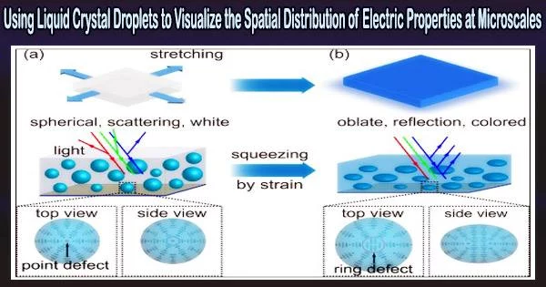
On this front, liquid crystal droplets (LCDs), micron-sized soft matter droplets with molecular orientational organization, fortunately, provide hope. Since LCDs have a strong response to outside stimuli like an electric field, they can function as a high-resolution probe.
Capitalizing on this promise, Dr. Shinji Bono and Prof. Satoshi Konishi from Ritsumeikan University, Japan, have now utilized LCDs for visualizing the electric properties of microstructured electrodes via a technique called particle imaging electrometry. Their findings were published in Volume 13 of the journal Scientific Reports on 16 March 2023.
The LCDs were dispersed on microelectrodes arranged in a comb-like structure atop a glass slab. Their molecular orientations, determined using polarized optical microscopy, were randomly distributed when the electric field was absent. Then, a voltage was applied across the electrodes.
Dr. Shinji Bono
Dr. Bono explains the research methodology. “The LCDs were dispersed on microelectrodes arranged in a comb-like structure atop a glass slab. Their molecular orientations, determined using polarized optical microscopy, were randomly distributed when the electric field was absent. Then, a voltage was applied across the electrodes.”
The LCDs in front of the electrode ends and between the electrodes rotated as a result, with their molecular orientations aligning perpendicularly and parallelly to the electrodes, respectively.
The researchers’ COMSOL simulations showed that this alignment followed the electric field’s direction and progressed more quickly with higher voltage. The relaxation frequency of rotation was found to vary as the square of the applied voltage.
Additionally, at high voltages, the LCDs displayed translation (linear motion) along the direction of the electrodes, particularly their endpoints, which are where the density of electrostatic charge is at its highest.
A micro-capacitive MEMS device’s energy density might be periodically modulated by the researchers to create an array of LCDs based on this characteristic. In turn, the LCD array worked as a periodic modulator of the refractive index, a measurement that describes a material’s capacity to bend light.
These findings show that one need only observe the rotational and translational behavior of LCDs in an electric field to examine the electric characteristics of microelectrodes and microelectric devices.
Moreover, the technique provides a high spatial resolution (10 μm) as well as high detection accuracy (5 μV/μm). Prof. Konishi has great expectations for its uses in light of these characteristics.
“It will help improve the design and fabrication of integrated microelectrical devices by providing information on the defect location, which so far has remained unavailable. In turn, more sophisticated MEMS technology may become available soon,” he concludes.