Semiconducting nanomaterials with 3D network architectures offer large surface areas and many pores, making them ideal for adsorption, separation, and sensing applications.
However, achieving outstanding functioning and end-use adaptability while simultaneously controlling electrical characteristics and constructing effective micro- and macro-scale structures remains a challenge.
Researchers from Osaka University have created a nanocellulose paper semiconductor in partnership with The University of Tokyo, Kyushu University, and Okayama University that allows for both nano-micro-macro trans-scale designability of 3D structures and extensive tunability of electrical properties. Their findings are published in ACS Nano.
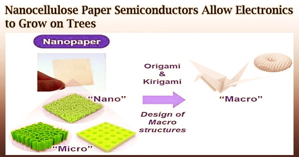
Cellulose is a wood-derived material that is both natural and easy to get by. Nanocellulose (cellulose nanofibers) can be manufactured into sheets of flexible nanocellulose paper (nanopaper) with A4-sized dimensions.
A basic electronic building block is usually packaged in a discrete form with two or more connecting leads or metallic pads. Individual components (such as resistors, capacitors, transistors, and diodes) or sophisticated sets of components (such as integrated circuits) can be packaged (as in the case of an operational amplifier, resistor array, or logic gate).
Although nanopaper does not conduct electricity, it can be made to do so by heating it. Unfortunately, the nanostructure can be disrupted as a result of this heat exposure.
We applied an iodine treatment that was very effective for protecting the nanostructure of the nanopaper. Combining this with spatially controlled drying meant that the pyrolysis treatment did not substantially alter the designed structures and the selected temperature could be used to control the electrical properties.
Hirotaka Koga
As a result, the researchers designed a treatment procedure that allows them to heat the nanopaper without causing damage to the paper’s structures from the nanoscale to the macroscale.
“An important property for the nanopaper semiconductor is tunability because this allows devices to be designed for specific applications,” explains study author Hirotaka Koga.
“We applied an iodine treatment that was very effective for protecting the nanostructure of the nanopaper. Combining this with spatially controlled drying meant that the pyrolysis treatment did not substantially alter the designed structures and the selected temperature could be used to control the electrical properties.”
The researchers employed origami (paper folding) and kirigami (paper cutting) techniques to demonstrate the nanopaper’s macro flexibility in a fun way. A bird and a box were folded, shapes like an apple and a snowflake were punched out, and laser cutting was used to create more elaborate constructions. This highlighted the level of detail attainable as well as the heat treatment’s lack of damage.
Nanopaper semiconductor sensors built into wearable devices to detect inhaled moisture breaking through facemasks and moisture on the skin are examples of successful uses. The nanopaper semiconductor was also employed as an electrode in a glucose biofuel cell, which generated enough energy to light a tiny lamp.
“The structure maintenance and tunability that we have been able to show is very encouraging for the translation of nanomaterials into practical devices,” says Associate Professor Koga. “We believe that our approach will underpin the next steps in sustainable electronics made entirely from plant materials.”