Indium antimonide (InSb) is a crystalline compound made from the elements indium (In) and antimony (Sb). It is part of the III-V group of semiconductors, which are formed by combining elements from group III (such as indium) and group V (such as antimony) of the periodic table. It has a narrow bandgap of about 0.17 eV at room temperature. This makes it an ideal material for certain applications in infrared (IR) detection and high-speed electronics.
It is a narrow-gap semiconductor material from the III-V group used in infrared detectors, including thermal imaging cameras, FLIR systems, infrared homing missile guidance systems, and in infrared astronomy. Indium antimonide detectors are sensitive to infrared wavelengths between 1 and 5 μm.
Indium antimonide was a very common detector in the old, single-detector mechanically scanned thermal imaging systems. Another application is as a terahertz radiation source as it is a strong photo-Dember emitter.
Properties
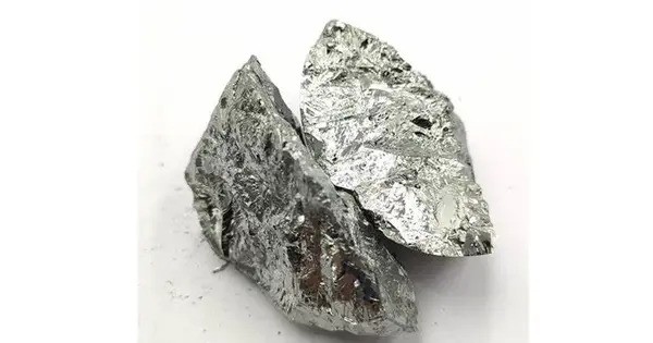
InSb has the appearance of dark-grey silvery metal pieces or powder with vitreous lustre. When subjected to temperatures over 500 °C, it melts and decomposes, liberating antimony and antimony oxide vapors. The crystal structure is zincblende with a 0.648 nm lattice constant.
- Chemical formula: InSb
- Molar mass: 236.578 g·mol−1
- Appearance: Dark grey, metallic crystals
- Density: 5.7747 g⋅cm−3[1]
- Melting point: 524 °C (975 °F; 797 K)[1]
- Band gap: 0.17 eV
- Electron mobility: 7.7 mC⋅s⋅g−1 (at 27 °C)
- Thermal conductivity: 180 mW⋅K−1⋅cm−1 (at 27 °C)
Electrical Properties
InSb is known for its high electron mobility, which is one of the highest among semiconductors. This makes it a good candidate for high-speed devices, especially in the context of high-frequency electronics.
Infrared Detection
Due to its narrow bandgap, InSb is particularly sensitive to infrared radiation. It is widely used in infrared detectors and imaging systems, such as in night vision devices and thermal cameras. InSb detectors are especially effective in the 3-5 micrometer infrared range.
Applications
- Infrared Detectors: As mentioned, InSb is extensively used in infrared detectors, particularly for military, medical, and scientific applications.
- High-Speed Electronics: InSb’s high electron mobility makes it suitable for high-frequency transistors, such as those used in radio-frequency (RF) applications, microwave devices, and fast-switching transistors.
- Quantum Devices: Due to its narrow bandgap and high electron mobility, InSb is also being explored for quantum computing and other quantum electronic applications.
- Photovoltaics: InSb can be used in photovoltaic cells, particularly for capturing infrared light and converting it into electrical energy.
Challenges
- Temperature Sensitivity: InSb’s performance can degrade at higher temperatures due to the narrowing of its bandgap. As a result, it is often used in applications where the device will operate at lower temperatures.
- Material Synthesis: Producing high-quality single-crystal InSb can be challenging due to its sensitivity to processing conditions, and defects can impair its performance.


