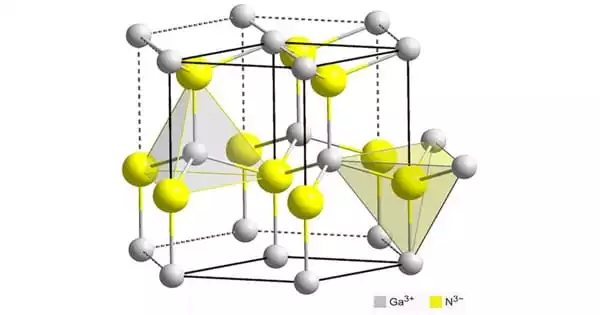
Gallium nitride (GaN) is a binary III/V direct bandgap semiconductor that has been used in blue light-emitting diodes since the 1990s. It is a direct bandgap semiconductor material used to make semiconductor devices such as transistors and diodes. The compound is a very hard material with a Wurtzite crystal structure. Its wide bandgap of 3.4 eV gives it unique properties for use in optoelectronics, high-power, and high-frequency devices. GaN, for example, is the substrate that enables violet (405 nm) laser diodes to be realized without the need for nonlinear optical frequency-doubling.
GaN has a particularly wide bandgap of 3.2 eV, allowing it to withstand extremely high voltages and operate at extremely high temperatures. It has a wide range of applications, from optoelectronic devices to high-frequency radio communications, and new applications for this efficient, highly powerful semiconductor material are constantly being discovered.
Its sensitivity to ionizing radiation is low (as is that of other groups III nitrides), making it a good material for satellite solar cell arrays. Military and space applications may benefit as well, as devices have demonstrated stability in radiation environments. GaN transistors are ideal power amplifiers at microwave frequencies because they can operate at much higher temperatures and voltages than gallium arsenide (GaAs) transistors. Furthermore, GaN has promising properties for THz devices. GaN is also emerging as a promising candidate for 5G cellular base station applications due to its high power density and voltage breakdown limits.
Physical properties
GaN is a mechanically stable, wide-bandgap semiconductor material with a high heat capacity and thermal conductivity. It is resistant to cracking in its pure form and can be deposited as a thin film on sapphire or silicon carbide, despite the mismatch in their lattice constants. GaN can be doped with silicon (Si) or oxygen to become n-type and magnesium (Mg) to become p-type. The Si and Mg atoms, on the other hand, alter the way GaN crystals grow, introducing tensile stresses and making them brittle. Gallium nitride compounds also have a high dislocation density, typically ranging from 108 to 1010 defects per square centimeter.
In 1999, the Army Research Laboratory (ARL) of the United States provided the first measurement of the high field electron velocity in GaN. ARL researchers achieved a peak steady-state velocity of 1.9 x 107 cm/s with a transit time of 2.5 picoseconds in an electric field of 225 kV/cm. The electron mobility was calculated using this information, providing data for the design of GaN devices.
Current GaN applications include:
- Lasers and photonics applications such as light-emitting diodes (LEDs),
- Solar cells for photovoltaic systems,
- Radiation-hardened transistors for satellites,
- Wireless power transmission,
- DC-DC converters for datacom applications, e.g. server farms and centralized telecommunications centers,
- Imaging and sensing, e.g. power amplifiers for microwave and terahertz (ThZ) devices.


