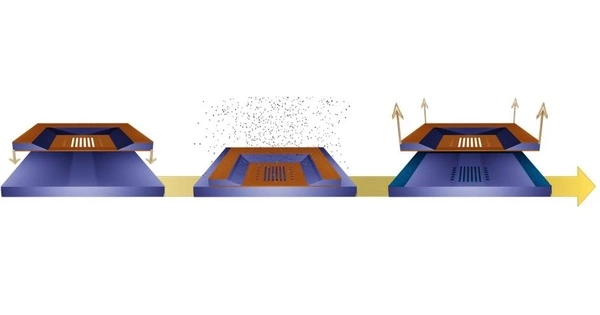
Stencil lithography is a novel method of creating nanometer scale patterns with nanostencils, which are stencils (shadow masks) with nanometer apertures. It is a patterning technique used in nano- and microfabrication. It is a resist-free, simple, parallel nanolithography process that requires no heat or chemical treatment of the substrates (unlike resist-based techniques). It is a type of lithography in which specific patterns on a substrate are defined using a stencil or mask.
The stencil used in stencil lithography is typically made of thin material, such as metal or polymer, with openings or cutouts in the desired shapes and sizes. The stencil is placed close to the substrate, and the pattern is transferred onto the substrate using a deposition or etching process.
History
S. Gray and P. K. Weimer published the first scientific paper on stencil lithography as a micro-structuring technique in 1959. During metal deposition, they used long-stretched metallic wires as shadow masks. Membranes can be made of a variety of materials, including metals, Si, SixNy, and polymers. At the full 4″ wafer scale, stencil apertures can now be scaled down to sub-micrometer size. This is known as a nanostencil. Laser interference lithography (LIL), electron beam lithography, and focused ion beam lithography were used to create nanoscale stencil apertures.
There are two main types of stencil lithography:
- Deposition Stencil Lithography: A stencil is used in this method to selectively deposit material onto the substrate. The stencil is placed on top of the substrate, and the deposited material, such as metals, polymers, or nanoparticles, is applied through the stencil’s openings. The stencil prevents material from being deposited in areas not covered by the openings, allowing for precise pattern transfer. Material deposition techniques include inkjet printing, spray coating, and evaporation.
- Etching Stencil Lithography: In this method, the stencil is used as a mask to protect certain areas of the substrate while etching or removing material from the uncovered regions. The stencil is placed on top of the substrate, and an etchant or reactive ion beam is applied to selectively remove material from the exposed areas. The stencil acts as a barrier, ensuring that the etching process is confined to the desired pattern.
Processes
Several processes are possible with stencil lithography, including material deposition and etching, as well as ion implantation. For the various processes, different stencil requirements are required, such as an extra etch-resistant layer on the backside of the stencil for etching (if the membrane material is sensitive to the etching process) or a conductive layer on the backside of the stencil for ion implantation.
Advantages
When compared to other lithographic techniques, such as photolithography or electron beam lithography, stencil lithography has several advantages. Because it does not require complex optics or expensive equipment, it is a relatively simple and cost-effective process. Stencils are simple to make using standard microfabrication techniques. Stencil lithography also enables large-area patterning, making it ideal for printed electronics, sensors, and microfluidics.
Limitations
However, stencil lithography has some drawbacks. It is typically limited to feature sizes in the micrometer range, making it unsuitable for nanoscale patterning. The final pattern resolution is determined by the stencil fabrication process, which may impose some constraints. To achieve accurate pattern transfer, stencil-to-substrate alignment is also required.


