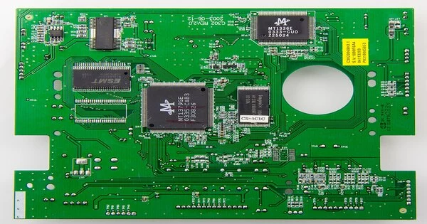
A stamped circuit board (SCB) is a type of printed circuit board that uses conductive pathways, tracks, or traces etched from copper sheets laminated onto a non-conductive substrate to mechanically support and electrically connect electronic components. It is a type of electronic circuit board that is made by stamping. This technology is used in the production of small circuits, such as LEDs. The circuit pattern is typically etched onto a copper-clad substrate using chemicals in traditional PCB manufacturing.
Stamped PCBs, on the other hand, form the circuit pattern by stamping or pressing conductive material onto the substrate. Similar to printed circuit boards this layer structure may comprise glass-fibre reinforced epoxy resin and copper. Basically, in the case of LED substrates three variations are possible:
- the PCB (printed circuit board),
- plastic-injection molding and
- the SCB.
The SCB technology can structure and laminate the most diverse material combinations in a reel-to-reel production process. Because the layers are structured separately, better design concepts can be implemented. As a result, heat dissipation from within the chip is much better and faster.
Production
Both the plastic and the metal are initially processed on separate reels, i.e. the materials are individually structured by stamping (“brought into form”) and then merged in accordance with the requirements.
The process of creating stamped circuit boards involves several steps:
- Substrate preparation: The base material, usually a non-conductive substrate such as fiberglass-reinforced epoxy, is prepared. It is often in the form of a large sheet or panel.
- Stamping tool preparation: A stamping tool or die is created, which contains the inverse image of the desired circuit pattern. The stamping tool is typically made of metal and may consist of multiple layers for complex circuit designs.
- Stamping process: The stamping tool is pressed onto the substrate with high pressure and sometimes heat, depending on the material being used. This causes the conductive material to be pressed onto the substrate, creating the circuit pattern.
- Finishing: After the stamping process, additional steps may be performed to complete the PCB manufacturing. This can include plating the conductive traces to enhance their durability and conductivity, drilling holes for component placement, and applying solder mask and silkscreen markings.
Advantages
The engineering choice of substrates is determined by the specific application, module design/substrate assembly, material, and thickness of the material involved.
Using these parameters, SCB technology can achieve good thermal management because rapid heat dissipation from beneath the chip means a longer service life for the system. Furthermore, SCB technology enables the material to be selected to meet the relevant requirements before optimizing the design to achieve a “perfect fit.”
Limitations
Stamped PCBs, on the other hand, may have limitations when it comes to complex circuitry with fine traces and close component spacing. The stamping process is not as precise as etching, and achieving the same level of detail and accuracy can be difficult.
Overall, stamped circuit boards are an alternative manufacturing method that can be appropriate for certain applications, providing cost and time advantages in some cases. The choice between stamped PCBs and traditional etched PCBs is determined by the circuit design and production needs.