A new technique has been developed that allows researchers to synthesize a perovskite solar material, characterize its crystal structure, and test its light response all at the same time. An exciting new solar material known as organic-inorganic halide perovskites may one day assist the United States in meeting its solar goals and decarbonizing the power grid. Perovskite solar materials, which are a thousand times thinner than silicon, can be tuned to respond to different colors of the solar spectrum simply by changing their composition mix.
Hybrid perovskite solar materials, which are typically made from organic molecules such as methylammonium and inorganic metal halides such as lead iodide, have a high tolerance for defects in their molecular structure and absorb visible light more efficiently than silicon, the solar industry’s standard.
Overall, these properties make perovskites promising active layers not only in photovoltaics (light-to-electricity technologies), but also in other types of electronic devices that respond to or control light, such as light-emitting diodes (LEDs), detectors, and lasers.
Although perovskites have great potential for greatly expanding solar power, they have yet to be commercialized because their reliable synthesis and long-term stability has long challenged scientists.
Carolin Sutter-Fella
“Although perovskites have great potential for greatly expanding solar power, they have yet to be commercialized because their reliable synthesis and long-term stability has long challenged scientists,” said Carolin Sutter-Fella, a scientist at Lawrence Berkeley National Laboratory’s Molecular Foundry, a nanoscience user facility (Berkeley Lab). “A path to perfect perovskites may be within reach now.”
According to a recent Nature Communications study co-led by Sutter-Fella, solar materials manufacturing could be aided by a sophisticated new instrument that uses two types of light – invisible X-ray light and visible laser light – to probe the crystal structure and optical properties of a perovskite material as it is synthesized.
“Typically, when people make solar thin films, they have a dedicated synthesis lab and need to go to another lab to characterize it; with our development, you can fully synthesize and characterize a material at the same time, at the same place,” she explained. Sutter-Fella assembled an international team of top scientists and engineers for this project, which involved equipping an X-ray beamline endstation with a laser at Berkeley Lab’s Advanced Light Source (ALS).
The new instrument’s highly intense X-ray light allows researchers to probe the crystal structure of the perovskite material and reveal details about fast chemical processes. It can be used, for example, to describe what happens in the second before and after a drop of a solidifying agent transforms a liquid precursor solution into a solid thin film.
At the same time, its laser can be used to generate electrons and holes (electrical charge carriers) in the perovskite thin film, allowing scientists to observe the response of a solar material to light, whether as a finished product or during the intermediate stages of material synthesis.
“Equipping an X-ray beamline endstation with a laser enables users to probe these complementary properties at the same time,” Sutter-Fella explained. This combination of simultaneous measurements could become part of an automated workflow for real-time monitoring of perovskites and other functional materials production for process and quality control.
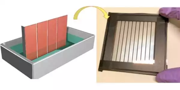
Spin coating is a low-cost technique that does not require expensive equipment or complicated chemical setups to produce perovskite films. The case for perovskites becomes even stronger when you consider how energy-intensive it is to simply manufacture silicon into a solar device – silicon requires a processing temperature of approximately 2,732 degrees Fahrenheit. Perovskites, on the other hand, can be easily processed from a solution at room temperature to 302 degrees Fahrenheit.
The beamline endstation enables researchers to observe what happens during synthesis, particularly during the first few seconds of spin coating, a critical time window during which the precursor solution slowly begins to solidify into a thin film.
As an ALS doctoral fellow, first author Shambhavi Pratap, who specializes in the use of X-rays to study thin-film solar energy materials, was instrumental in the development of the instrument. She recently completed her doctoral studies in the Müller-Buschbaum group at the Technical University of Munich.
“The instrument will allow researchers to document how small things that are normally taken for granted can have a significant impact on material quality and performance,” Pratap said. “Everything matters when it comes to making reproducible and efficient solar cells at a low cost,” Sutter-Fella explained. She went on to say that the study was a collaborative effort involving a wide range of scientific disciplines.
Sutter-Fella received a Berkeley Lab Early Career Laboratory Directed Research and Development (LDRD) Award in 2017 for this work, which is the latest chapter in a body of work. “We know the research community is excited about using this new capability at the ALS,” she said. “Now we want to make it more user-friendly so that more people can benefit from this endstation.”