Researchers were actively looking into materials other than silicon for the fabrication of transistors. Due to their superior electrical properties and ability to operate at higher frequencies and temperatures, materials such as gallium nitride (GaN) and silicon carbide (SiC) were gaining traction.
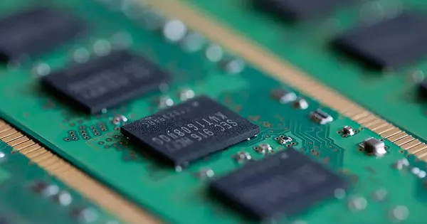
Transistors with variable properties are critical components in the development of tomorrow’s semiconductors. As standard transistors approach their size limit, having more functions on the same number of units becomes increasingly important in enabling the development of small, energy-efficient circuits for improved memory and more powerful computers. Lund University in Sweden researchers demonstrated how to create new configurable transistors and exert control on a new, more precise level.
There is a lot of interest in reconfigurable transistors because there is a constant need for better, more powerful, and efficient circuits. The advantage of these is that, unlike standard semiconductors, the properties of the transistors can be changed after they have been manufactured.
Scaling down the size of silicon transistors has historically improved the computational power and efficiency of computers (also known as Moore’s Law). However, the costs of continuing development along those lines have risen significantly, and quantum mechanics issues have slowed progress.
The goal is to create neuromorphic circuits, which are circuits adapted for artificial intelligence because their structure is similar to the human brain with its synapses and neurons.
Anton Eriksson
Instead, new materials, components, and circuits are being sought. Lund University is a world leader in III-V materials, which are a silicon substitute. These are materials with significant potential for use in the development of high-frequency technology (for example, parts for future 6G and 7G networks), optical applications, and increasingly energy-efficient electronic components.
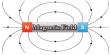
To realize this potential, ferroelectric materials are used. When exposed to an electric field, these special materials can change their inner polarization. It is similar to a regular magnet, but instead of a magnetic north and south pole, electric poles with a positive and negative charge on each side of the material are formed. By changing the polarisation, it is possible to control the transistor. Another advantage is that the material “remembers” its polarization, even if the current is turned off.
Through a new combination of materials, the researchers have created ferroelectric “grains” that control a tunnel junction — an electrical bridging effect – in the transistor. This is on an extremely small scale — a grain is 10 nanometres in size. By measuring fluctuations in the voltage or current, it has been possible to identify when polarisation changes in the individual grains and thus understand how this affects the transistor’s behaviour.
New ferroelectric memory in the form of transistors with tunnel barriers was investigated in order to create new circuit architectures, according to the newly published research.
“The goal is to create neuromorphic circuits, which are circuits adapted for artificial intelligence because their structure is similar to the human brain with its synapses and neurons,” says Anton Eriksson, who recently completed his doctorate in nanoelectronics.
The new findings are notable in that tunnel junctions were created using ferroelectric grains located directly adjacent to the junction. These nanograins can then be controlled individually, whereas previously only entire groups of grains, known as ensembles, could be tracked. In this way, it is possible to identify and control separate parts of the material.
“In order to create advanced applications, you must first understand the dynamics in individual grains down to the atomic level, as well as the defects that exist. The increased understanding of the material can be used to optimise the functions. By controlling these ferroelectric grains, you can then create new semiconductors in which you can alter properties. By changing the voltage, you can thus produce different functions in one and the same component,” says Lars-Erik Wernersson, professor of nanoelectronics.
The researchers have also examined how this knowledge can be used to create different reconfigurable applications by manipulating in various ways the signal that goes through the transistor. It could, for example, be used for new memory cells or more energy-efficient transistors.
This new transistor is known as a ferro-TFET, and it can be used in both digital and analog circuits.
“What’s interesting is that the input signal can be modulated in a variety of ways, such as by the transistor shifting phase, frequency doubling, and signal mixing.” “Because the transistor remembers its properties even when the current is turned off, there’s no need to reset it every time the circuit is used,” explains Zhongyunshen Zho, a doctoral student in nanoelectronics.
Another advantage of these transistors is their ability to operate at low voltage. This makes them energy-efficient, which will be necessary in future wireless communication, the Internet of Things, and quantum computers.