Engineers created a new artificial intelligence chip with the goal of developing sustainable, modular electronics. The chip can be reconfigured, with layers that can be swapped out or stacked on to add new sensors or updated processors, for example.
Consider a more sustainable future in which cellphones, smartwatches, and other wearable devices are not required to be stored or discarded in favor of a newer model. Instead, they could be upgraded with cutting-edge sensors and processors that snap onto a device’s internal chip, much like LEGO bricks incorporated into an existing structure. Such reprogrammable chipware could keep devices current while reducing electronic waste.
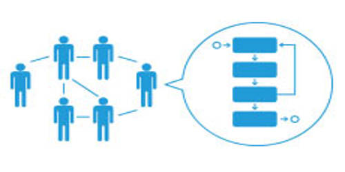
With a LEGO-like design for a stackable, reconfigurable artificial intelligence chip, MIT engineers have taken a step toward that modular vision. The chip’s layers communicate optically thanks to alternating layers of sensing and processing elements, as well as light-emitting diodes (LED). Other modular chip designs use traditional wiring to transfer signals between layers. Because such intricate connections are difficult, if not impossible, to sever and rewire, stackable designs cannot be reconfigured.
The MIT design transmits data through the chip using light rather than physical wires. As a result, the chip can be reconfigured, with layers that can be swapped out or stacked on top, for example, to add new sensors or updated processors.
“You can add as many computing layers and sensors as you want, such as for light, pressure, and even smell,” says Jihoon Kang, an MIT postdoc. “We call this a LEGO-like reconfigurable AI chip because the combination of layers allows for infinite expandability.”
As we enter the era of the internet of things based on sensor networks, demand for multifunctioning edge-computing devices will expand dramatically. Our proposed hardware architecture will provide high versatility of edge computing in the future.
Jeehwan Kim
The researchers are eager to apply their design to edge computing devices, which are self-contained sensors and other electronics that operate independently of any central or distributed resources, such as supercomputers or cloud computing.
“As we enter the era of the internet of things based on sensor networks, demand for multifunctioning edge-computing devices will expand dramatically,” says Jeehwan Kim, associate professor of mechanical engineering at MIT. “Our proposed hardware architecture will provide high versatility of edge computing in the future.”
The team’s results are published in Nature Electronics. In addition to Kim and Kang, MIT authors include co-first authors Chanyeol Choi, Hyunseok Kim, and Min-Kyu Song, and contributing authors Hanwool Yeon, Celesta Chang, Jun Min Suh, Jiho Shin, Kuangye Lu, Bo-In Park, Yeongin Kim, Han Eol Lee, Doyoon Lee, Subeen Pang, Sang-Hoon Bae, Hun S. Kum, and Peng Lin, along with collaborators from Harvard University, Tsinghua University, Zhejiang University, and elsewhere.
Lighting the way
The design of the team is currently configured to perform basic image recognition tasks. It accomplishes this through the use of a layering of image sensors, LEDs, and processors made from artificial synapses — arrays of memory resistors, or “memristors,” developed previously by the team, which function as a physical neural network, or “brain-on-a-chip.” Without the need for external software or an Internet connection, each array can be trained to process and classify signals directly on a chip.
The researchers combined image sensors with artificial synapse arrays, which they trained to recognize specific letters – in this case, M, I, and T – in their new chip design. While a conventional approach would be to relay a sensor’s signals to a processor via physical wires, the team instead fabricated an optical system between each sensor and artificial synapse array to enable communication between the layers, without requiring a physical connection.

“Other chips are physically wired through metal, making them difficult to rewire and redesign, so you’d need to make a new chip if you wanted to add any new function,” MIT postdoc Hyunseok Kim explains. “We replaced that physical wire connection with an optical communication system, which allows us to stack and add chips however we see fit.”
The optical communication system developed by the team is made up of paired photodetectors and LEDs, each patterned with tiny pixels. Photodetectors serve as an image sensor for receiving data and LEDs serve as data transmitters to the next layer. As a signal (for instance an image of a letter) reaches the image sensor, the image’s light pattern encodes a certain configuration of LED pixels, which in turn stimulates another layer of photodetectors, along with an artificial synapse array, which classifies the signal based on the pattern and strength of the incoming LED light.
Stacking up
The team created a single chip with a computing core about 4 square millimeters in size, or about the size of confetti. The chip is made up of three image recognition “blocks,” each of which includes an image sensor, an optical communication layer, and an artificial synapse array for classifying one of three letters: M, I, or T. They then shone a pixellated image of random letters onto the chip and measured the electrical current produced by each neural network array. (The higher the current, the more likely the image is the letter that the particular array has been trained to recognize.)
The researchers discovered that the chip correctly classified clear images of each letter, but it was less capable of distinguishing between blurry images, such as I and T. The researchers were able to quickly replace the chip’s processing layer with a better “denoising” processor, and the chip then correctly identified the images.
“We demonstrated stackability, replaceability, and the ability to insert a new function into the chip,” says Min-Kyu Song, an MIT postdoc. The researchers intend to expand the chip’s sensing and processing capabilities, and they envision limitless applications.
“We can add layers to a cellphone’s camera so it can recognize more complex images, or we can turn these into healthcare monitors that can be embedded in wearable electronic skin,” says Choi, who previously developed a “smart” skin for monitoring vital signs with Kim. Another concept he proposes is modular chips built into electronics that consumers can customize with the latest sensor and processor “bricks.”
“We can create a general chip platform and sell each layer separately, like a video game,” Jeehwan Kim says. “We could create various types of neural networks, such as for image or voice recognition, and let the customer choose what they want to add to an existing chip, much like a LEGO.”