Historical Overview:
In 1839 a French physicist first discovered the photovoltaic effect while experimenting with an electrolytic cell made up of two metal electrodes. [45] After, the first intentional PV device was developed by the American inventor Charles Fritts in 1883. He melted selenium into a thin sheet of on a metal substrate and pressed gold-leaf film as the top contact. Later on, in 1954 researchers at Bell Labs accidentally discovered that p-n junction diodes generated a voltage when the room lights were on. Within a year they had produced a 6% efficient silicon p-n junction solar cell. The same efficiency was achieved the same year by the group at Wright Patterson air force base in the USA, only this time, they used a thin-film hetero-junction solar cell based on Cu2S/CdS. By the year 1960, several documents were written showing different solar cells built using different materials for the p-n junction, some key documents written by Prince, Loferski, Rappaport and Wysoski, Shockley and Queisser developed the fundamentals of p-n junction cell operation including the theoretical relationship between band gap, incident spectrum, temperature, thermodynamics and efficiency [46]. In the years to come the US and the USSR space programs played an important role in the R&D of solar cells, since they were the main energy source to power their satellites. The year 1973 was very important for PV technological advancement. First the “violet cell” was developed, having an improved short wavelength response leading 30% relative increase in efficiency over the most advanced silicon cells at that time. Also, the same year an important event occurred called the Cherry hill conference. During this event a group of PV researchers and heads of US government scientific organizations met to evaluate the scientific merit and potential of photovoltaics. The outcome was the decision that photovoltaic’s was worthy of government support, resulting in the formation of the US Energy Research and Development Agency, the world’s first government group setup whose mission included fostering research on renewable energy, which ultimately became the US dept of Energy. Finally in October, the first oil crisis pressed all the governments worldwide to encourage the use of renewable sources of energy, especially solar. [46] From this point, solar research had the momentum and funding it needed from fuel providers, electric utilities and other interested parties to make a real impact on the energy industry. However, this didn’t last long because in 1982 the public funding was cut by the national governments worldwide. It is due to this withdrawal of support that has left the impression that solar power cannot succeed without substantial subsidies. Yet progress did not stop, it just switched direction and rapid changes in the technology and PV industry and parties interested took place to begin a transformation of the energy industry. All around the world energy sustainability was getting more attention because of energy security issues and climate change. But the reasons for these sustainable changes should not only be attributed to social environmental consciousness. The main driving factor, as with almost all emerging industries, is economic sensibility. At the same time the fossil fuel industry was experiencing problems with supply and cost, China’s economy was developing at incredible rates. As of 2005, for example, China accounted for almost 30% of global growth where the European community accounted for just 5%. And as China develops, the amount of oil needed for economic expansion is comparatively more per unit of growth [47]. All of this indicates that even with the most optimistic view of conservation programs, sustainable energy generation will have to increase if development is expected to continue at current rates. Fortunately a healthy mix of sustainable energy generation technologies along with the gradual phasing out of widespread fossil fuel use is one likely scenario for the future. However, the most recent expansion of solar power is occurring mainly in Germany and Japan. At first glance this might seem surprising since neither Germany or Japan have a large amount of sunlight, but their lack of fossil fuel sources combined with a national government committed to sustainable energy programs have enabled solar power to thrive. Together these two countries, with Japan’s sunshine program and Germany’s 100.000 solar roofs program along with several government subsidies account for a full 69% of the world market for PV as of 2005. Also, the rate at which this market is expanding is encouraging – from 85 MW in 1995 to 1.1 GW globally in 2005.
Technology:
The smallest entity within a PV system is a solar cell. The solar cell is a semi conductor device, more precisely, a special type of diode. Incident lights free electrons. They are separated by an internal electromagnetic field as a consequence of the potential difference at the p-n junction. Voltage is generated between both surface contacts and a connected load draws a current fig (23). [49, 50].
As its name implies, photovoltaic is a technology that converts light (photo) directly into electricity (voltaic). The name of the individual photovoltaic element is known as solar cell, which is made out of materials called semiconductors. The most used semiconductor material is silicon, which in its naturally occurring state has the unique property of 4 electrons in its outer orbit, allowing them to form perfect covalent bonds with four neighboring atoms, thus creating a lattice. The obtained crystalline form is a silvery, metallic looking substance. In its pure state, crystalline silicon is a poor conductor, due to the fact that all of the electrons in the
outer orbit are bonded and cannot freely move. To change this behavior, pure silicon has to go through a process called doping. In this process some “impurities” (e.g. C, N, As, B) are added to the material [48].
A number of different solar cell technologies are currently applied or under development (Table 1). More than 90% of today’s annual solar production is made from crystalline silicon (figure 10). However, other semiconductor materials are also applied and several technologies are investigated [30].
According to the type of material added, the semiconductor receives the P or N classification.
● N-Type: Arsenic or phosphorous is added and since each element has 5 electrons in their outer orbit, there is one electron that has nothing to bond to, therefore is free to move within
the material. By adding several atoms of arsenic or phosphorous, enough electrons will be able to move, allowing an electrical current to flow through the material. The name “n-type”
comes from the electron’s negative charge.
● P-type: Boron or gallium is added. In this case each one has only 3 outer orbit electrons, and when added to pure silicon, there is a hole in the structure where one silicon electron has
nothing to bond to and is free to move. The absence of electrons creates the effect of positive charge, hence the “p-type” name . These electrons are occupying a band of energy called
the valence band. When some energy is applied and exceeds a certain threshold, called the band gap, these electrons are free to move in a new energy band called the conduction band, where they can conduct electricity through the material. The energy required for the electrons to migrate to the conduction band can be provided by photons which are particles of light. Figure 1 shows the idealized relationship between energy (vertical axis) and the spatial boundaries (horizontal axis). When the solar cell is exposed to sunlight, photons hit the electrons in the valence band and give them enough energy to migrate into the conduction band. There, a n-doped semiconductor contact collects the conduction-band electrons and drives them to the external circuit where they can be used to create electricity. Then they are restored to the valence band at a lower (free) energy through the return circuit by a p-doped semiconductor contact.
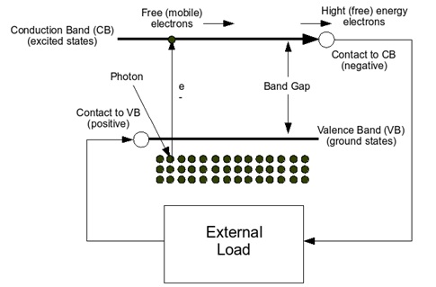
Figure (23): Schematic of solar cell [30]
This is all possible because sunlight is a spectrum of photons distributed over a wide range of energy. Photons with greater energy than the band gap can drive electrons from the valence band to the conduction band and can travel through the external circuit to produce work. Photons with less energy than the band gap cannot excite the free electrons, and instead, that energy travels through the solar cell and is absorbed as heat. The voltage at which electrons are delivered to the external circuit are slightly less than the band gap. This voltage is measured in units of electron volts (eV), thus in a material with 1eV band gap the voltage delivered by a single cell is around 0.7V. Therefore multiple cells are connected together and encapsulated into units called PV modules which is the product usually sold to the customer.
Wafer –type Crystalline Silicon Cells:
Crystalline silicon cells are usually manufactured from silicon wafers. The wafers are sawn out of single or multicrystalline silicon ingots by means of wire saws. Typically
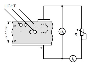
Figure (24): Schematic representation of crystalline solar cell supplying a resistive load.
They are about 0.3mm thick. A single crystalline wafer is in fact one single crystal. Multicrystalline silicon is composed of large crystal grains. Multicrystalline silicon cells are
Slightly cheaper, but have a somewhat lower efficiency. A relatively new approach is the production of multicrystalline silicon wafer ribbons or sheets, saving the cost of wafering ingots and reducing the sawing losses. Depending on the process applied, the frequency of ribbon of solar cells varies from little lower than up to comparable to that of multicrystalline cells [52]
To transform a silicon cell wafer into a solar cell, it is subjected to a number of steps, the most prominent being.
– Surface cleaning and etching and possibly surface texturing,
– Doping, for instance, by phosphorous diffusion,
– Attachment of front and back metal contacts, typically by screen printing,
– Deposition of antireflection coating.
Crystalline wafer-type silicon cells are expected to dominate the world market at least for the current data
Table: Overview of the application solar-cell technologies.
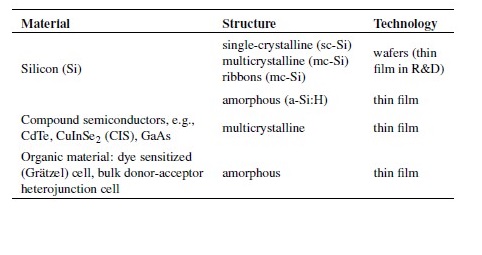
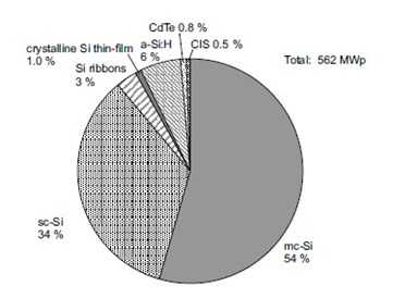
Figure (25): Market share of different cell technologies in 2002 [36]
![]()
Figure (26): I-U curve of a crystalline silicon photovoltaic cell.
Crystalline:
Crystalline Silicon technology (c-Si) accounts for more than 90% of the actual PV systems in the market, the reason why its presence is so high it’s because it has use all the technology and R&D of the semiconductors for the electronics industry since the 1960’s. Furthermore, silicon is one of the most abundant minerals in the earth’s crust, giving refineries virtually unlimited supply resources. However, silicon is a very brittle material, requiring relatively thick cells (~300um, although 100um thick cells can be obtained using the latest sawing technology), therefore some of the electrons excited by the photons have to travel large distances inside the materials, losing energy in a process called recombination, where electrons return to their valence band. Consequently a material with high purity and structural perfection is required. To avoid this loss, the electrons must be highly mobile, as they are in pure silicon. Imperfections and impurities can absorb the electron’s energy and convert it into heat, impeding the electron’s ability pass through an electric circuit. Once silicon of the desired purity is obtained, it is then put together into ingots and then cut into wafers using a saw. Wafers stand for about 65% of the module cost, equally divided between purification, crystallization and sawing. For many years the PV industry have used scrap silicon from the IC industry, but the increase of PV demand has nearly exhausted this market. The Siemens
method for obtaining silicon is the most used worldwide but it has been considered ultimately too expensive for its use in PV. The purity it provides, however, is well above what is necessary for the fabrication of solar cells.
Thin Films
Around 10 times more crystalline silicon is needed to absorb a given fraction of sunlight compared to other semiconductors like GaAs, CdTe, Cu (InGa)Se2 since silicon is the weakest absorbing semiconductor used for solar power. Therefore, thicker wafers have to be made when working with crystalline technologies and, because of the size, higher quality material has to be used because of the longer paths the high-energy electrons have to travel before reaching the external circuit. During the same years c-Si PV cells were developed, it was shown that other semiconductors could be used for electricity production. When this material is used to make solar cells, so little of this material is required that a foreign material is needed to physically support the cells. During the first years of thin-films development, 4 technologies achieved higher efficiencies than 10%, Cu2S/CdS, 21 a-Si, CuInSe2/CdS and CdTe/CdS. Cu2S/CdS disappeared soon due to stability problems related to electrochemical decomposition. The main advantage of the thin films is the lower price they could achieve once set into a mass production scheme.
Thin-film solar cell consist of a thin layer of electrically active semiconductor material, deposited on a cheap substrate. They offer a high potential for cost reduction due to their low material requirement [52]. Today they are mainly applied for consumer products and small stand-alone applications. Thin-film modules for power applications are not yet considerably cheaper than crystalline modules. By 2010, different thin-film technologies are expected to become a valuable alternative for wafer-type silicon. Nevertheless, they are not expected to replace wafer type silicon cells yet
Organic solar cells are based on organic semiconductors. Organic solar cells are not yet commercially available. However, in the long run, they may contribute to further reduce the cost of PV modules after the cost-reduction potential of inorganic thin-films will have been exploited[52].
This work does not focus on PV cell technology, but on the application of PV in grid-connected systems. The following investigations on PV system aspects implicitly assume the application of crystalline cells. Due to the dominance of crystalline silicon cells in the world market, this approach is reasonable. Nevertheless, most results may also be extended to other types of PV cells.
Electrical properties
The electrical properties of PV devices are given at so-called standard test conditions (STC):
– Cell temperature: 250 C;
– SOLAR IRRADIANCE: 1000W/M ;
– Solar spectrum: Air Mass 1.5.
The power maximum under STC is called peak power and it is indicated by the index p . Isc and Uoc are short-circuiting current and open-circuit voltage, respectively. MPP stands for maximum power point and indicates the point on the I-U curve where the generated power reaches its maximum. Rated values of current, voltage and power are generally given at the MPP under STC. A typical I-U curve of a crystalline silicon PV cell is provided in Figure 11. The open-circuit voltage of a crystalline silicon cell decreases with increasing temperature with about 0.4% of UMPP under STC per Kelvin. Simultaneously, the short-circuit current increases proportionally to the solar irradiance.
Solar-cell Efficiency
The efficiency under STC is defined as the ratio of peak power to cell area times irradiance under STC. Depending on the applied area, efficiencies found in the literature vary significantly. Today, efficiency values of small crystalline silicon cells in the laboratory can be as high as 25% under STC [54]. The parameter efficiency mainly shows the state of the art of different cell production technologies and serves as a benchmark for the achieved progress in solar-cell research.
Applied to PV system, the efficiency mainly expresses the power generation normalized to surface area. For the description of system performance and energy yield, the concept of efficiency is usually not applied.
Photovoltaic Modules
In order to make PV easy to handle in practice, solar cells are assembled into PV modules. Inside the module, the cells are connected in series and parallel by means of copper strips in order to achieve practically applicable voltage and current. Mechanical and optical properties are ensured by the physical structure, chosen for the particular module. Additionally, the module structure protects the cells and conductors from humidity. The typical sandwich structure of a PV module is shown in figure 26.
As front cover low-iron glass is used in order to minimize absorption. The interconnected cells are embedded between EVA (ethyl vinyl acetate) sheets or in cast resin in order to protect them from mechanical stress. In standard modules, the back side is usually covered by the aluminium- Tedler layer. Tedler is a trademark for polyvinyl fluoride (PVF). The aluminium- Tedler layer protects the modules from moisture and ensures cooling of the solar cells, due to its high conductivity. Glass is applied when the back side of the modules is desired to be transparent at the cost of reduced cooling of the solar cells and higher weight of the module.
Glass-Tedler modules typically are standard modules, produced in large quantities. They are mostly framed with aluminium for easier mounting; however, frameless glass-Tedler modules do exist. Frameless modules are called laminates.
Glass-Tedler modules typically are standard modules, produced in large quantities. They are mostly framed with aluminium for easier mounting; however, frameless glass-Tedler mo0dules to exist. Frameless modules are called laminates.
Glass-glass modules are mainly applied in building-integrated PV. There, they may be used as building element, for example, for awnings or structural glazing.
Standard PV modules are often classified as 12 or 24V Modules with 36 or 72 solar cells, respectively, in series. The MPP voltage of a crystalline silicon cell under STC is slightly less than 0.5V,as a consequence of appropriate doping. Consequently, the MPP voltage of such modules under STC is a little less than 18 or 36V, respectively. Historically, these specifications became the standard case because such a module still exhibits a voltage, high enough to load a 12 or 24V battery, even in bad circumstances such as low irradiance and high cell temperature. In order to make sure that all solar cells in one string have the same MPP current, for module production solar cells are usually screened and sorted according to their efficiency or even their I-U curves [55].
If single solar cells inside a module are shadowed,
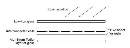 Figure (27): Schematic cross section of a photovoltic module assembly
They may become reverse-biased by the voltage of the remaining unshadowed cells of the series connection. In order to prevent shadowed cells from reverse bias and consecutive breakdown, each substring of typically 18 series-connected solar cells is equipped with an ant parallel diode. The so-called bypass diodes are usually situated in the terminal box at the module’s back side. A thorough literature review with regard to shadowing and the function of the bypass diodes is available in [56].
From a survey of the German market in 2003 it appears that the lion’s share of standard modules for grid-connected applications is rated in the range of 100 to 180Wp per module. The rating varies with the size and efficiency of the applied solar cells and the number of parallel cell strings within a module. The module efficiency under STC is roughly situated between 11 and 15%.
For power applications, photovoltaic modules are typically assembled in larger groups in order to provide the desired power rating at a specified DC voltage. In order to yield the required DC voltage, modules are first connected in series into strings of modules. Subsequently, strings of equal voltage rating can be connected in parallel to a DC bus in order to achieve the required rated power. The parallel connection of strings occurs in a generator junction box where the necessary safety equipment may also be located. The assembly of PV array is to be emphasized; the term PV generator is also applied.
Equivalent circuit and characteristics equation:
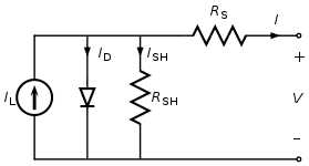
Figure (28): The equivalent circuit of a solar cell
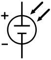
Figure: The schematic symbol of a solar cell
To understand the electronic behavior of a solar cell, it is useful to create a model which is electrically equivalent, and is based on discrete electrical components whose behavior is well known. An ideal solar cell may be modeled by a current source in parallel with a diode; in practice no solar cell is ideal, so a shunt resistance and a series resistance component are added to the model. The resulting equivalent circuit of a solar cell is shown on the left. Also shown, on the right, is the schematic representation of a solar cell for use in circuit diagrams.
Characteristic equation
From the equivalent circuit it is evident that the current produced by the solar cell is equal to that produced by the current source, minus that which flows through the diode, minus that which flows through the shunt resistor:
I = IL − ID − ISH
where
- I = output current (amperes)
- IL = photo generated current (amperes)
- ID = diode current (amperes)
- ISH = shunt current (amperes)
The current through these elements is governed by the voltage across them:
Vj = V + IRS
Where
- Vj = voltage across both diode and resistor RSH (volts)
- V = voltage across the output terminals (volts)
- I = output current (amperes)
- RS = series resistance (Ω)
By the Shockley diode equation, the current diverted through the diode is:
![]()
Where
- I0 = reverse saturation current (amperes)
- n = diode ideality factor (1 for an ideal diode)
- q = elementary charge
- k = Boltzmann’s constant
- T = absolute temperature
- At 25°C,
 volts
volts
By Ohm’s law, the current diverted through the shunt resistor is:
![]()
Where
- RSH = shunt resistance (Ω)
Substituting these into the first equation produces the characteristic equation of a solar cell, which relates solar cell parameters to the output current and voltage:
![]()
An alternative derivation produces an equation similar in appearance, but with V on the left-hand side. The two alternatives are identities; that is, they yield precisely the same results.
In principle, given a particular operating voltage V the equation may be solved to determine the operating current I at that voltage. However, because the equation involves I on both sides in a transcendental function the equation has no general analytical solution. However, even without a solution it is physically instructive. Furthermore, it is easily solved using numerical methods. (A general analytical solution to the equation is possible using Lambert’s W function, but since Lambert’s W generally itself must be solved numerically this is a technicality.)
Since the parameters I0, n, RS, and RSH cannot be measured directly, the most common application of the characteristic equation is nonlinear regression to extract the values of these parameters on the basis of their combined effect on solar cell behavior
Open-circuit voltage and short-circuit current:
When the cell is operated at open circuit, I = 0 and the voltage across the output terminals is defined as the open-circuit voltage. Assuming the shunt resistance is high enough to neglect the final term of the characteristic equation, the open-circuit voltage VOC is:
![]()
Similarly, when the cell is operated at short circuit, V = 0 and the current I through the terminals is defined as the short-circuit current. It can be shown that for a high-quality solar cell (low RS and I0, and high RSH) the short-circuit current ISC is:
![]()
Simple diagram of Electricity generation by Cell:
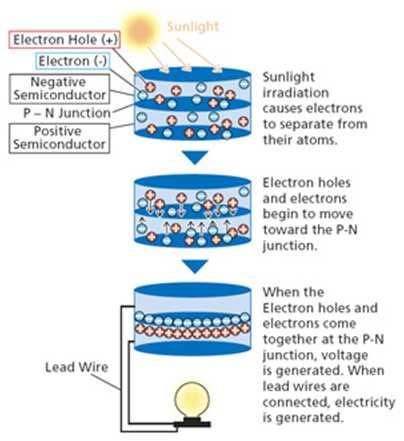 Sunlight irradiation causes electrons to separate from their atoms. Electron holes and electrons begin to move toward the P-N junction. When the electron holes come together at the P-n junction, voltage is generated. When the lead wires are connected, electricity is generated.


