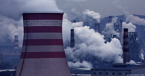
Berkeley Lab has developed a cost-effective thermoelectric waste-heat recovery system with a $2 million grant from the California Energy Commission (CEC) to reduce electricity-related carbon emissions. High-temperature waste heat is emitted by industries such as glass, cement, power, and steel. Converting this waste heat to electricity at a low cost can provide a zero-carbon energy source.
The system is based on silicon nanowires developed several years ago at Berkeley Lab. “Developing thermoelectric generators from an abundant and inexpensive material like silicon will increase market penetration while assisting industries in minimizing energy losses,” said Berkeley Lab scientist Vi Rapp.
The funding comes from the CEC’s Electric Program Investment Charge (EPIC) program, which supports clean energy innovation in order to reduce pollution, promote economic development, and meet the state’s climate goals. Every year, roughly 45 quads of energy are rejected as waste heat at high temperatures (greater than 300 degrees Celsius) around the world. For comparison, the United States uses about 100 quads of primary energy each year.
Berkeley Lab Scientists developed a cost-effective thermoelectric waste-heat recovery system to reduce electricity-related carbon emissions.
Berkeley Lab research was focused on the low-temperature conversion of waste heat to electricity more than ten years ago, which was a significant technological advancement at the time. Because converting waste heat at high temperatures is cost-effective and competitive with other zero-carbon and waste heat conversion technologies, high-temperature thermoelectric conversion has been identified as the next sought-after technological advancement.
A Berkeley Lab and Stanford team was funded by the CEC to find a promising solution, and their findings were recently published in the journal Nature Communications. The team created a technology that uses wafer-scale arrays of porous silicon nanowires with ultra-thin silicon crystallite to achieve an 18-fold higher “figure of merit” (a performance or efficiency expression) than other high-temperature or bulk silicon thermoelectric technologies.
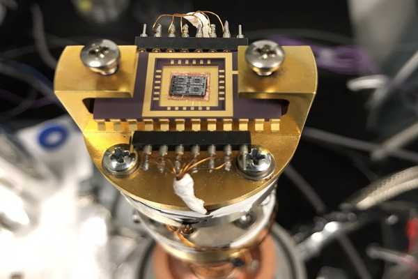
High-temperature thermoelectrics can cost-effectively convert waste heat and compete with other zero-carbon technologies. Among the various high-temperature thermoelectric materials, silicon nanowires have the advantage of being both cost-effective and having mature manufacturing infrastructures. Despite significant advances in thermoelectrics based on silicon nanowires for waste heat conversion, the figure of merit (ZT) or operating temperature has remained low.
It will most likely work for Silicon nanowires used in TEGs (thermoelectric generators). The main issue with TEGs has always been their inefficiency. If the heat you’re harvesting is of sufficient quality (that is, hot enough) to be used in another heat engine, it will almost certainly be more efficient than using a TEG, so the only advantage of a TEG is that there are no moving parts to wear out. However, there are other wear-out mechanisms for TEGs that run too hot. As a result, most TEGs will have a temperature limit for long-term use. Generally, you’d want to use them where the temperature isn’t high enough to make other methods more effective, or where other heat engines aren’t warranted, such as using an ICE’s exhaust gases to generate a bit of electrical power.
One of the drawbacks of using nanowires is that the layer is so thin that it cannot support a large temperature difference across it. Maybe you can use a lot of layers to provide the thermal insulation (while still allowing electrical conduction) that is required here, but I don’t see this as economically viable. However, there may be some applications where it is more useful than other technologies.
“High temperatures degrade materials,” said Ravi Prasher, the project’s lead and an Energy Technologies Area scientist at Berkeley Lab. “So we looked at silicon, which is abundant, stable, cheap, and dependable. Because bulk silicon has poor thermoelectric properties, we use it to make nanowires, which alters the physics.”
The next step, according to Prasher, will be to scale up the system by producing nanowires to test in actual devices.

