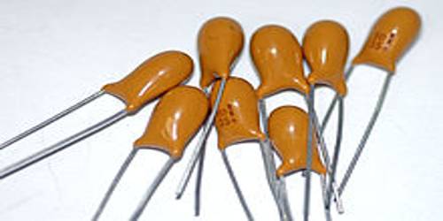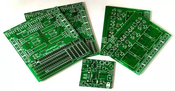
A printed circuit board is a medium for connecting electronic components in a controlled manner. It is a laminated sandwich structure of conductive and insulating layers with an artwork pattern of traces, planes, and other features etched from one or more sheet layers of copper laminated onto and/or between sheet layers of a non-conductive substrate.
A PCB is made up of multiple layers of different materials. The core layer is composed of an insulating substrate, which is typically FR-4 (a flame-retardant epoxy fiberglass composite). A thin layer of copper is laminated on top of this core layer, and a photosensitive material known as the solder mask is applied on top of the copper layer to protect it from oxidation and provide insulation.
Electrical components can be soldered to conductive pads on the outer layers in the shape designed to accept the component’s terminals to electrically connect and mechanically fasten them to it. Vias are plated-through holes that allow interconnections between layers in another manufacturing process.
Printed circuit boards are found in almost all electronic devices. Wire wrap and point-to-point construction were once popular but are now rarely used as alternatives to PCBs. PCBs necessitate more design work to lay out the circuit, but manufacturing and assembly can be automated.
Much of the layout work can be automated using electronic design automation software. Because components are mounted and wired in a single operation, mass-producing circuits with PCBs is less expensive and faster than other wiring methods. A large number of PCBs can be manufactured at the same time, and the layout only needs to be done once. PCBs can also be produced manually in small quantities, albeit with diminished benefits.
The PCB design is created using computer-aided design (CAD) software, specifying the placement of components and the routing of electrical connections. Once the design is finalized, it goes through a fabrication process involving the following steps:
- Substrate Preparation: The core layer is prepared by cleaning and coating it with a thin layer of copper.
- Imaging: A photosensitive material called the photoresist is applied over the copper layer. The PCB design is then printed onto a transparent film or photomask. The film is aligned with the core layer, and ultraviolet light is used to expose the photoresist through the photomask, creating a pattern of hardened and unhardened areas.
- Etching: The unhardened areas of the photoresist are removed, leaving behind the pattern of copper traces. The board is then placed in an etching solution, typically containing chemicals like ferric chloride, which selectively dissolve the exposed copper, leaving only the desired copper traces.
- Solder Mask Application: A solder mask layer is applied over the entire surface of the PCB, except for the areas where the copper traces and component pads are exposed. The solder mask helps prevent solder bridges and provides insulation between the conductive traces.
- Component Placement: Electronic components, such as resistors, capacitors, integrated circuits, and connectors, are placed on the PCB according to the design specifications. This can be done manually or using automated assembly machines.
- Soldering: The components are soldered onto the PCB to establish electrical connections. This can be done using wave soldering, reflow soldering, or hand soldering techniques, depending on the complexity of the circuit and the production requirements.
- Testing and Inspection: The assembled PCB is tested for functionality and inspected for any defects or manufacturing errors. Various testing methods, such as automated optical inspection (AOI) and in-circuit testing (ICT), are employed to ensure the quality of the PCB.
After passing the testing phase, the PCB can be integrated into electronic devices or systems. PCBs range in complexity from simple single-layer boards used in basic electronics to multi-layer boards with intricate designs used in advanced applications such as computer motherboards or smartphones.