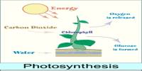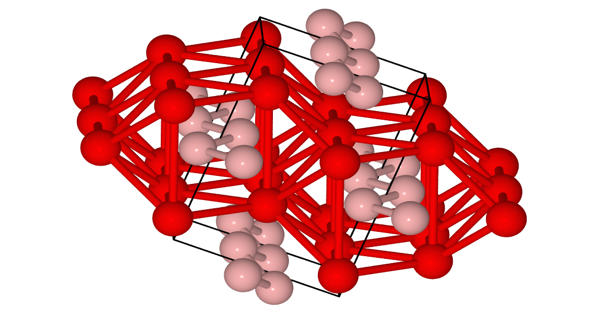
Nickel monosilicide is an intermetallic compound formed out of nickel and silicon. Alloying elements can substantially affect the formation and morphological stability of nickel monosilicide. Like other nickel silicides, NiSi is of importance in the area of microelectronics.
Preparation
Nickel monosilicide can be prepared by depositing a nickel layer on silicon and subsequent annealing. A method for fabricating a layer including nickel monosilicide on a substrate including silicon. It has been well recognized as a promising silicide for future ULSI devices. In the case of Ni films with thicknesses above 4 nm, the normal phase transition is given by Ni2Si at 250°C followed by NiSi at 350 °C and NiSi2 at approximately 800 °C. The method includes the steps of incorporating, on a portion of the thickness of the substrate comprising silicon, an element selected from W, Ti, Ta, Mo, Cr and mixtures thereof; depositing, on the substrate, a layer of nickel and a layer of an element selected from Pt, Pd, Rh, and mixtures thereof or a layer comprising both nickel and an element selected from Pt, Pd, Rh, and mixtures thereof; heating to a temperature sufficient for obtaining the formation of a layer comprising nickel silicide optionally in the form of nickel monosilicide NiSi; incorporating fluorine in the layer; and optionally, heating to a sufficient temperature to convert the layer to a layer comprising nickel silicide entirely in the form of nickel monosilicide NiSi.
It can have low resistivity of 15 μΩ cm on deep submicron lines and after high temperature (>600°C) annealing. For ultra-thin nickel films, with thicknesses below 4 nm, nickel monosilicide is formed at lower annealing temperatures of 230–290 °C. converted into the mono-silicide (NiSi), without agglomeration, by low-temperature (400-600/spl deg/C) rapid thermal annealing.
Uses
Several properties make NiSi an important local contact material in the area of microelectronics, among them a reduced thermal budget, low resistivity of 13–14 μΩ·cm, and a reduced Si consumption when compared to alternative compounds. A nickel-monosilicide (NiSi) technology suitable for a deep sub-micron CMOS process has been developed. It has been confirmed that a nickel film sputtered onto n/sup +/- and p/sup +/-single-silicon and polysilicon substrates are uniformly. This NiSi technology was used in the experimental fabrication of deep-sub-micrometer CMOS structures; the current drivability of both n- and p-MOSFET’s was higher than with the conventional titanium silicide process, and the ring oscillator constructed with the new MOSFET’s also operated at higher speed.
Information Source: