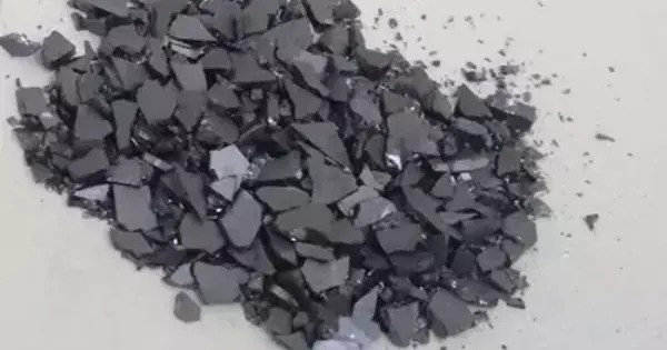
Indium phosphide (InP) is a binary semiconductor composed of indium and phosphorus. It is primarily used in high-speed electronics and optoelectronics, particularly in applications like high-frequency transistors, photodetectors, and laser diodes due to its excellent electronic properties and performance in the infrared region. It has a face-centered cubic (“zincblende”) crystal structure, identical to that of GaAs and most of the III-V semiconductors.
Manufacturing
Indium phosphide can be prepared from the reaction of white phosphorus and indium iodide at 400 °C., also by direct combination of the purified elements at high temperature and pressure, or by thermal decomposition of a mixture of a trialkyl indium compound and phosphine.
Properties
Indium Phosphide is a crystalline solid, typically appearing as a gray or brown powder. InP has a high melting point around 1,200°C (2,192°F). It is relatively hard and brittle, making it susceptible to cracking under mechanical stress.
- Chemical formula: InP
- Molar mass: 145.792 g/mol
- Appearance: black cubic crystals
- Density: 4.81 g/cm3, solid
- Melting point: 1,062 °C (1,944 °F; 1,335 K)
- Solubility: slightly soluble in acids
- Band gap: 1.344 eV (300 K; direct)
- Electron mobility: 5400 cm2/(V·s) (300 K)
- Thermal conductivity: 0.68 W/(cm·K) (300 K)
Applications
The application fields of InP splits up into three main areas. It is used as the basis for optoelectronic components, high-speed electronics, and photovoltaics.
Natural Occurrence
InP does not naturally occur in significant quantities as a mineral. Instead, its occurrence is mostly in the form of industrial by-products or in materials used for electronic and optoelectronic device manufacturing.
Industrial Production
The commercial production of indium primarily comes from the processing of zinc ores, and while the main use of indium is in thin-film technology (such as in Indium Tin Oxide or ITO for touchscreens), it also plays a significant role in the manufacture of InP. The global production of indium is limited, and the cost of indium has led to efforts to recycle and reuse indium from various electronic waste sources.
High-speed optoelectronics
InP is used as a substrate for epitaxial optoelectronic devices based other semiconductors, such as indium gallium arsenide. The devices include pseudomorphic heterojunction bipolar transistors that could operate at 604 GHz.
Optical Communications
InP is used in lasers, sensitive photodetectors and modulators in the wavelength window typically used for telecommunications, i.e., 1550 nm wavelengths, as it is a direct bandgap III-V compound semiconductor material. The wavelength between about 1510 nm and 1600 nm has the lowest attenuation available on optical fibre (about 0.2 dB/km). Further, O-band and C-band wavelengths supported by InP facilitate single-mode operation, reducing effects of intermodal dispersion.


