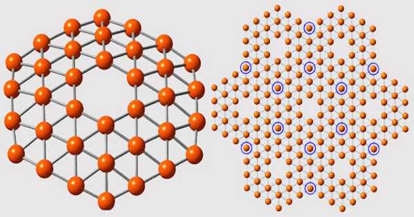
Borophene is a two-dimensional allotrope of boron that is also known as boron sheet. It is a crystalline atomic monolayer of boron. Different borophene structures were experimentally confirmed in 2015, after being predicted by theory in the mid-1990s.
Northwestern University engineers have created a double layer of atomically flat borophene for the first time, defying boron’s natural tendency to form non-planar clusters beyond the single-atomic-layer limit.
Despite its promising electronic properties, borophene – a single-atom-layer-thick sheet of boron is difficult to synthesize. Unlike its two-dimensional analog graphene, which can be peeled away from naturally layered graphite with something as simple as scotch tape, borophene cannot be peeled away from bulk boron. Borophene must instead be grown directly on a substrate.
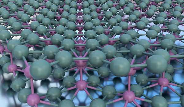
If growing a single layer of atomically flat borophene was difficult, growing multiple layers of atomically flat borophene seemed impossible. Growing boron beyond single atomic layers results in clustering rather than planar films because bulk boron is not layered like graphite.
Engineers have created a double layer of atomically flat borophene, a feat that defies the natural tendency of boron to form non-planar clusters beyond the single-atomic-layer limit.
Borophenes have ideal strength and in-plane elasticity. In some configurations, they can be stronger than graphene and more flexible. Boron nanotubes, for example, have a higher 2D Young’s modulus than any other known carbon or noncarbon nanostructure. Because of the fluxional nature of their multi-center in-plane bonding, borophenes undergo novel structural phase transitions under in-plane tensile loading. Because of its high theoretical specific capacities, electronic conductivity, and ion transport properties, borophene has the potential to be used as an anode material for batteries.
“When you try to grow a thicker layer, the boron wants to adopt its bulk structure,” said Mark C. Hersam, co-senior author of the study at Northwestern. “Thicker boron films, rather than remaining atomically flat, from particles and clusters. The key was to identify growth conditions that prevented cluster formation. We didn’t think you could go beyond one layer until now. We have now entered uncharted territory between the single atomic layer and the bulk, resulting in a new playground for exploration.”
The research is published in the journal Nature Materials.
Hersam is the Walter P. Murphy Professor of Materials Science and Engineering and the director of the Materials Research Science and Engineering Center at the McCormick School of Engineering. He is also a member of the International Institute for Nanotechnology and the Simpson Querrey Institute at Northwestern. Boris Yakobson, the Karl F. Hasselmann Chair in Engineering at Rice University, and Hersam co-led the project.
Hersam and his colleagues discovered borophene for the first time five years ago. Borophene, which is stronger, lighter, and more flexible than graphene, has the potential to transform batteries, electronics, sensors, solar cells, and quantum computing. Although theoretical research predicted the possibility of a double layer of borophene, many researchers, including Hersam, were skeptical.
“It’s difficult to create new materials, even when theoretical work predicts their existence,” Hersam said. “Theory almost never tells you the synthetic conditions required to achieve that new structure.”
The substrate used to grow the material, Hersam’s team discovered, was the key to the proper conditions. Hersam and his colleagues grew borophene on a flat silver substrate for the study. When subjected to extremely high temperatures, the silver clumped together to form exceptionally flat, large terraces between clusters of atomic-scale steps.
“We saw a second layer forming when we grew borophene on these large, flat terraces,” Hersam explained. “Following that fortuitous observation, we purposefully directed our efforts in that direction. When we discovered the second layer, we weren’t looking for it. Many materials discoveries are made in this manner, but you must recognize the opportunity when you come across something unexpected.”
The double-layered material retained all of the desired electronic properties of borophene while adding new benefits. For example, the material could be made up of two atomic-layer-thick sheets bonded together with space in between and used for energy or chemical storage.
“Theoretical predictions indicate that bilayer borophene is a promising material for batteries,” Hersam said. “The space between the layers provides a place for lithium ions to accumulate.” Hersam’s team hopes that this work will inspire other researchers to grow even thicker layers of borophene or to create double layers with different atomic geometries.
“Diamonds, graphite, graphene, and carbon nanotubes are all based on the same element (carbon) but have different geometries,” Hersam explained. “Boron appears to have just as many possibilities as carbon, if not more. We think we’re still in the early stages of the two-dimensional boron saga.”