Although most of us find nanotechnology and materials science to be complicated subjects, research in these fields is critical to almost everyone. Your electronic devices, for example, are completely reliant on it.
Semiconductors are now used in all microelectronics. These are materials that do not conduct electricity well. However, tiny amounts of other substances can be added to them, a process known as doping. This improves semiconductor performance, making them not so bad after all.
“Previously, we didped semiconductors and saw that this drastically changed the electrical properties of the material,” says Ph.D. candidate Kasper Aas Hunnestad of NTNU’s Department of Materials Science and Engineering. This is all very well. It’s wonderful when something works. But, aside from the fact that it works, we haven’t always understood why it works. At the atomic level, this is especially true.
“We now understand much better how to image the individual added atoms, which were previously nearly impossible to find. This provides us with new information and allows us to understand how they affect the properties of that material” Hunnestad adds.
Conventional microscopy techniques didn’t allow us to observe how small amounts of additives positioned themselves in semiconductors. The new results show that the investment in the very best technical equipment, such as this APT machine, pays off enormously and makes ground-breaking research possible.
Hunnestad
Why ‘knowing why’ is important, too
What’s the big deal? Why should we be concerned with single atoms and why something works? Isn’t it enough just to know that it works? If this were the case, physicists and chemists would have a lot of fun doing the research, but the rest of us would get very little out of it.
“Only when you understand how something works can you manipulate and optimize it,” Dennis Meier says. He is the project’s director and a professor in the Department of Materials Science and Engineering at NTNU.
This way, for example, you can make more efficient, environmentally friendly, or cheaper materials for the job to be done. Or you can assign new properties to a material that you already have available with much greater precision. This is also key for developing future materials for sustainable technology.
“Often, we want to introduce new functionality to materials. For that we need to know exactly what role each individual atom plays,” says Meier.
Advanced imaging techniques make it possible
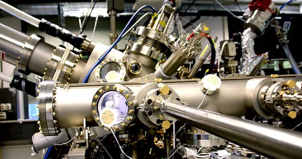
In a recent article in Nature Communications, Hunnestad and colleagues present the results of many, many hours of work using “atom probe tomography” (APT). APT is a sophisticated piece of cutting-edge technology that NTNU acquired a few years ago. According to Constantinos Hatzoglou, the machine can provide a three-dimensional representation of what a material looks like down to the atomic level. He works as a senior engineer in the Department of Materials Science and Engineering’s APT laboratory.
Hunnestad and colleagues took advantage of this exceptional capability to investigate a new type of oxide-based semiconductor to which very small amounts of a substance were added to tailor its properties.
“Conventional microscopy techniques didn’t allow us to observe how small amounts of additives positioned themselves in semiconductors,” says Hunnestad. The new results show that the investment in the very best technical equipment, such as this APT machine, pays off enormously and makes ground-breaking research possible.
Shows the enormous potential
The research is still not exactly easy using APT either. But by bringing together colleagues with different experimental and theoretical backgrounds—along with hard and inspired work—the NTNU team has found solutions.
“This isn’t just a wonderful achievement. It also shows the enormous potential of the APT technique for research fields where it has not been applied before. It shows the unique opportunities we have thanks to the modern infrastructure available in NTNU’s NanoLab and TEM Gemini Center,” says Meier.
Hunnestad has worked with APT for about three years. He has carried out extensive correlated microscopy measurements, supported by Antonius van Helvoort and Per Erik Vullum. Van Helvoord is a professor at NTNU’s Department of Physics and experts in high-resolution electron microscopy, while Vullum is a professor II at NTNU, Department of Physics and senior researcher at SINTEF Industry.
Hunnestad and Meier are enthusiastic about all the fascinating possibilities that have already emerged from their APT-based research and the novel perspectives for the characterization of functional materials at the atomic scale.
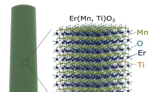
Imaging of individual titanium atoms mixed into a semiconductor
The researchers examined the oxide-based semiconductor Er(Mn,Ti)O3 for their recent article. Their collaborators at the Lawrence Berkeley National Laboratory in the United States added trace amounts of titanium (Ti) to erbium manganate for this purpose (ErMnO3).
“We can get a three-dimensional representation of how the titanium atoms are positioned in the semiconductor using the atom probe,” Meier says. “This allows us to link the material’s new electrical properties all the way down to individual atoms.”
Dr. Muhammad Zeeshan Khalid is a member of the team led by Sverre Selbach, an associate professor in the Department of Materials Science and Engineering at NTNU. He added calculations to the experiments. These calculations give us a better understanding of the effects that individual atoms can have on physical properties.
One advantage of the researchers’ work is that the method can be applied to a wide range of other substances. It is not limited to the substances with which the NTNU research team has experimented.
“The procedures and outcomes are of general interest. They can help us learn more about oxide-based semiconductors and functional materials in general. The study opens up entirely new avenues” Meier explains.