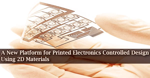
Scientists have demonstrated how electricity travels through printed 2D materials, paving the possibility for the development of flexible medical devices and other applications.
The physical principles responsible for the transfer of electricity in printed two-dimensional (2D) materials are revealed in a study led by Imperial College London and Politecnico di Torino researchers, which was published today in Nature Electronics.
The research determines which features of 2D material films must be modified in order to produce electrical devices on-demand, enabling for the rational design of a new class of high-performance printed and flexible electronics. Most of our devices, from fitness trackers to cellphones, are powered by silicon chips.
Their inflexible rigidity, on the other hand, hinders their application in flexible electronics. 2D materials, which are made up of single-atom-thick layers, can be distributed in solution and formed into printable inks, resulting in ultra-thin films that are very flexible, semi-transparent, and have novel electronic capabilities.
This opens the door to new sorts of electronics, such as those that may be embedded in flexible and elastic materials like clothing, paper, or even human tissues.
Researchers have previously constructed various flexible electronic devices from printed 2D material inks, but these were one-off ‘proof-of-concept’ components designed to demonstrate how one specific attribute, such as high electron mobility, light sensing, or charge storage, may be realized.
The fundamental understanding of how the electrons are transported through networks of 2D materials underpins the way we manufacture printed electronic components. By identifying the mechanisms responsible for such electronic transport, we will be able to achieve the optimum design of high-performance printed electronics.
Renato Gonnelli
However, their broad application has been limited because to a lack of understanding of which parameters to manage in order to construct printed 2D material devices.
Changes in temperature, magnetic field, and electric field regulate how electronic charge is conveyed in numerous inkjet-printed films of 2D materials, according to the multinational study team.
The researchers looked at three different types of 2D materials: graphene (a ‘semimetal’ made up of a single layer of carbon atoms), molybdenum disulphide (or MoS2, a ‘semiconductor’), and titanium carbide MXene (or Ti3C2, a metal), and mapped how the electrical charge transport changed under various conditions.
Lead researcher Dr. Felice Torrisi, from the Department of Chemistry at Imperial, said: “Our results have a huge impact on the way we understand the transport through networks of two-dimensional materials, enabling not only the controlled design and engineering of future printed electronics based on 2D materials, but also new types of flexible electronic devices.”
“For example, our work paves the way to reliable wearable devices suitable for biomedical applications, such as the remote monitoring of patients, or bio-implantable devices for long-term monitoring of degenerative diseases or healing processes.”
Invasive methods, such as implanting brain electrodes to monitor degenerative disorders that damage the nervous system, may be replaced by these future gadgets. Electrodes are only transitory and painful for the patient, whereas a flexible device composed of biocompatible 2D materials might be merged with the brain and enable continuous monitoring.
Wearable gadgets for monitoring healthcare, similar to fitness watches but better integrated with the body, could provide enough reliable data to allow doctors to follow patients without sending them to the hospital for tests.
Other researchers will be able to develop printable and flexible 2D material devices with the properties they desire, based on how they need the electrical charge to act, thanks to the correlations the team uncovered between 2D material type and the controls on electrical charge transit.
They may also disclose how to create whole new types of electrical components that are impossible to create with silicon chips, such as transparent components or those that change and transmit light in novel ways.
Co-author Professor Renato Gonnelli, from the Politecnico di Torino, Italy, said: “The fundamental understanding of how the electrons are transported through networks of 2D materials underpins the way we manufacture printed electronic components. By identifying the mechanisms responsible for such electronic transport, we will be able to achieve the optimum design of high-performance printed electronics.”
Co-first author Adrees Arbab, from the Cambridge Graphene Centre and the Department of Chemistry at Imperial, said: “In addition, our study could unleash the new electronic and optoelectronic devices exploiting the innovative properties of graphene and other 2D materials, such as incredibly high mobility, optical transparency, and mechanical strength.”


