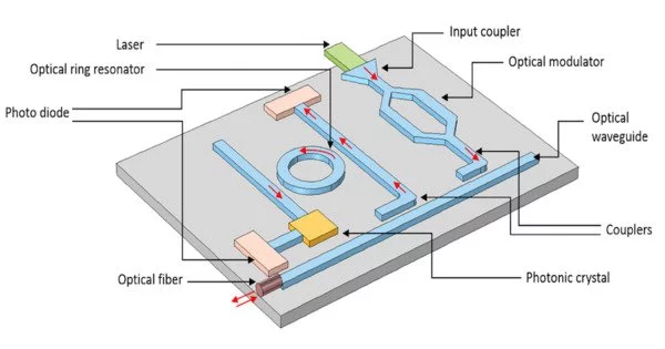
Silicon photonics is the study and application of photonic systems that use silicon as an optical medium. Silicon is typically patterned with sub-micrometre precision into microphotonic components. These operate in the infrared, most commonly at the 1.55 micrometre wavelength used by most fiber optic telecommunication systems. The silicon is typically layered on top of a layer of silica in what is known as silicon-on-insulator (SOI) construction (by analogy with a similar construction in microelectronics).
Electrical signals are used to transmit and process information in traditional electronic circuits. However, as data rates continue to rise, electronic components are being hampered by issues such as power consumption, heat dissipation, and signal degradation. Photonic technologies, on the other hand, use light to transmit and process data, allowing for high bandwidth, low latency, and immunity to electromagnetic interference.
Silicon photonic devices can be created using existing semiconductor fabrication techniques, and because silicon is already used as the substrate for most integrated circuits, hybrid devices with optical and electronic components integrated onto a single microchip are possible.
Silicon photonics takes advantage of the electronics industry’s mature semiconductor fabrication processes to create integrated optical components on a silicon substrate. This method allows for the integration of photonic devices such as lasers, modulators, detectors, and waveguides on a single chip alongside electronic components.
As a result, many electronics manufacturers, including IBM and Intel, as well as academic research groups, are actively researching silicon photonics as a means of staying on track with Moore’s Law by using optical interconnects to provide faster data transfer both between and within microchips.
The key advantages of silicon photonics include:
- Compatibility with existing CMOS fabrication processes: Silicon photonics takes advantage of the semiconductor industry’s well-established manufacturing infrastructure. This compatibility enables mass production at a low cost and integration with electronic circuits.
- High-speed data transfer: Silicon photonics enables data transmission at extremely fast rates, up to several terabits per second. This makes it appropriate for data centers, telecommunications, and high-performance computing.
- Compact size and scalability: The integration of photonic and electronic components on a single chip reduces system size. Furthermore, the technology is highly scalable, allowing for the integration of many optical components on a single chip.
- Energy efficiency: Silicon photonics offers improved energy efficiency compared to traditional electronic circuits, resulting in reduced power consumption and heat dissipation. This efficiency is especially important in data centers and other energy-sensitive applications.
Silicon photonics has been used in a variety of applications, including data communication, optical interconnects, high-performance computing, sensing, LiDAR systems, and biomedical devices. Ongoing research and development in the field is looking into new techniques, materials, and device architectures to improve the performance and capabilities of silicon photonics-based systems.