Electronics experts have recently given carbon nanotubes a lot of attention. Carbon nanotubes are enormous, cylindrical molecules made of hybridized carbon atoms organized in a hexagonal pattern. These special molecules can be used to make smaller field-effect transistors (FETs) with high energy efficiency because of their favorable electrical properties and geometric structure.
Although carbon nanotube-based FETs have the potential to beat smaller silicon-based transistors in practical applications, this has not yet been shown.
A recent paper by researchers at Peking University and other institutes in China, published in Nature Electronics, outlines the realization of FETs based on carbon nanotubes that can be scaled to the same size of a 10 nm silicon technology node.
“Recent progress in achieving wafer-scale high density semiconducting carbon nanotube arrays brough us one step closer to the practical use of carbon nanotubes in CMOS circuits,” Zhiyong Zhang, one of the researchers who carried out the study, told Phys.org. “However, previous research efforts have mainly focused on the scaling of channel or gate length of carbon nanotube transistors while keeping large contact dimensions, which cannot be accepted for high density CMOS circuits in practical applications.”
“Our primary objective of this work is to explore the true scaling capability of carbon nanotube arrays using two figures of merit in silicon industry, that is, contacted gate pitch and area of 6T SRAM cell, while maintaining the performance advantages.”
Zhang and his colleagues essentially set out to demonstrate the practical value of carbon nanotube transistors, showing that they can outperform conventional silicon-based FETs with a comparable gate pitch and a 6T SRAM cell area.
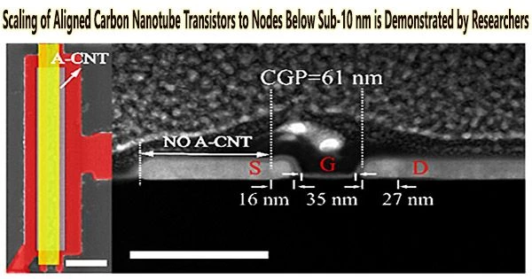
To do this, scientists initially created FETs with a contacting gate pitch of 175 nm that were built on arrays of carbon nanotubes. This gate pitch was realized by scaling the gate length and contact length to 85 nm and 80 nm, respectively.
This new contact scheme enables carbon nanotube transistors to be further downscaled to contacted gate pitch below 55 nm that corresponds to silicon 10 nm technology node, while outperforming 10 nm node silicon transistors due to high carrier mobility and Fermi velocity. Our work experimentally demonstrated a true 90 nm node technology using carbon nanotubes, which could be made geometrically smaller and offer electronic performance outperforming silicon 90 nm node transistors.
Zhiyong Zhang
“Remarkably, the transistors exhibited an impressive on-current of 2.24 mA/μm and a peak transconductance of 1.64 mS/μm, surpassing the electronic performance of silicon 45 nm node transistors,” Zhang said. “In addition, 6T SRAM cell consisted of these ultra-scaled nanotube transistors has been fabricated within 1 μm2, and functions correctly. We then investigated the major obstacle, that is, the contact resistance of carbon nanotube transistors for further scaling.”
Charge carriers can only be injected from the surface of carbon nanotubes when using the common contact method known as “side contact,” according to previous research. As a result, the nanotubes’ resistance is length dependant, which limits how small they can be made.
To overcome this issue, Zhang and his colleagues introduced a new scheme that they refer to as “full contact.” This method involves breaking the carbon nanotubes at both ends before making the contact, allowing some of the carriers to be injected from these ends.
“This new contact scheme enables carbon nanotube transistors to be further downscaled to contacted gate pitch below 55 nm that corresponds to silicon 10 nm technology node, while outperforming 10 nm node silicon transistors due to high carrier mobility and Fermi velocity,” Zhang said.
“Our work experimentally demonstrated a true 90 nm node technology using carbon nanotubes, which could be made geometrically smaller and offer electronic performance outperforming silicon 90 nm node transistors.”
In a recent publication, a trustworthy method for downscaling carbon nanotube transistors without affecting their performance was presented. The team’s approach has so far resulted in a transistor with a 90 nm node, but they believe that by redesigning the connections, similar transistors might be made with nodes as small as 10 nm or even smaller.
In the future, the work by Zhang and his colleagues could contribute to the creation of increasingly smaller and efficient carbon nanotube-based transistors. This could have valuable implications for the development of electronics.
“The next challenge that we are now tackling is to scale down the contact geometry for carbon nanotube n-type transistors to constructing complete CMOS technology, which is the necessary building blocks for modern digital ICs,” Zhang added.
“Currently, we use scandium for the contact of n-type carbon nanotube transistors. However, we are facing great difficulties as we scale down the contact length due to the oxidation of this low-work function metal. In addition, we are working to accurately characterize the interface quality between carbon nanotube arrays and high-κ dielectric, improving it to the level of silicon CMOS transistors to enhance gate controllability and reliability.”