| CHAPTER 1 |
COMPONENT INTRODUCTION
SYSTEM OVERVIEW:
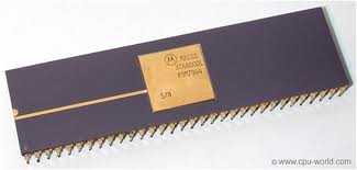
The 6800 is an 8-bit microprocessor produced by Motorola and released shortly after the Intel 8080 in late 1974. It had 78 instructions, including the (in)famous, undocumented Halt and Catch Fire (HCF) bus test instruction. It may have been the first microprocessor with an index register. It was usually packaged in a 40 pin DIP (dual-inline package).
 Figure1.1: Motorola 6800 Microprocessor.
Several first-generation microcomputers of the 1970s, available by mail order as kits or in assembled form, used the 6800 as their CPU; examples are the MEK6800D2 development board, the SWTPC 6800 (the first computer to use the 6800), the Heath kit ET-3400 Microprocessor Trainer, the MITS Altair 680 range (MITS offered these as alternatives to its Altair 8800 which used the Intel 8080), several of the Ohio Scientific designs, Gimix, Smoke Signal Broadcasting, Midwest Scientific, and the Newbear 77-68.
The 4051, a professional grade desktop graphical system intended for user programming in BASIC, was manufactured and sold by Tektronix. This integrated a 6800 processor, memory card, storage display tube, keyboard, and magnetic tape cassette in a single unit and employed an external thermal imaging printer for hard copy.
The 6800 ‘fathered’ several descendants, the pinnacle being the greatly extended and semi-compatible 6809, which was used in the Vectrex video game console and the TRS-80 Color Computer, among several others. There are also many microcontrollers descended from the 6800 architecture, such as the Motorola 6801/6803, 6805, RS08, 68HC08, 68HC11 and 68HC12.
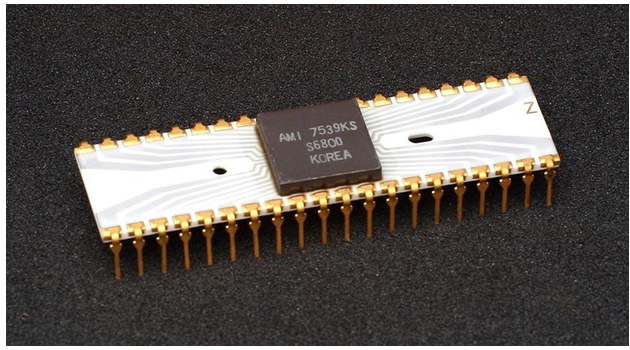
Figure: The AMI S6800 is a Motorola MC6800 clone.
Hitachi, Ltd. acted as a second source for many of Motorola’s CPUs, and also produced its own derivatives including the 6301 and 6303, which could run 6800 code. These microprocessors also had a couple of extra instructions added to their instruction sets.
Competitor MOS Technology came up with an architectural relative of the 6800, with its 6502 (‘lawsuit compatible’ MPU) and its successors. The 6502 did not have the 16-bit registers of the 6800, but had more addressing modes and was substantially cheaper. The 6502 was used in many computers and game consoles during the late 1970s and early-to-mid-1980s .
The 6800, used in the Sphere 1 personal computer, was supplanted by the Motorola 68000, used in large numbers in the Commodore Amiga and Apple Macintosh families before the introduction of the PowerPC, a RISC technology developed by IBM and produced jointly with Motorola.
MOTOROLA MICROOPROCESOR FAMILY:
The 6800 family of 8-bit microprocessors (µPs) and microcontrollers (µCs) is based upon the Motorola 6800 CPU. The architecture also inspired the MOS Technology 6502, and that company initially started business producing 6800 clones.The chips primarily competed against Intel’s 8-bit family of chips (such as the 8080, or their relations, the ZiLOG Z80 range).
| Microprocessors | Year |
| MOTOROLA 6800 | 1974 |
| MOTOROLA 68000 | 1979 |
| MOTOROLA 68020 | 1984 |
| MOTOROLA 68030 | 1987 |
| MOTOROLA 68040 | 1991 |
| MOTOROLA POWER PC 603 | 1993 |
| MOTOROLA 68060 | 1994 |
| MOTOROLA POWER PC 603 | 1994 |
| MOTOROLA POWER PC 604 | 1994 |
| MOTOROLA POWER PC 620 | 1996 |
MOTOROLA 6800 MICROOPROCESOR FAMILY:
Motorola’s initial microprocessor introduction was the 6800 in 1975. It was strictly an 8-bit processor capable of addressing 64 kilobytes of memory. Probably the most striking difference between the Motorola and Intel architectures is that early members of the 6800 family tended to minimize register usage in favor of general purpose RAM.
Motorola introduced numerous variations of the 6800. The 6802 incorporated 128 bytes of RAM on the CPU itself. The 6803/6808 ran faster (3.58 MHz), incorporated 128 bytes of RAM, and included both a URAT (universal asynchronous receiver or transmitter) for serial communications, and a counter/timer. The last variation of the 8-bit Motorola family was the 6809. It was similar to the 6802, but offered an enhanced instruction set, including what was probably the first multiply instruction on an 8-bit CPU.
Some of the earliest personal computer kits were based on the 6800 family, and Tandy built a version of the Color Computer that was rather advanced (for its day) around a 6809. However, by 1978, the age of the 16-bit CPU had begun, and the second generation of personal computers that included the Apple Macintosh and the IBM PC would be 16-bit machines.
MOTOROLA 680X0 MICROPROCESOR FAMILIES:
In the mid 1970s at Motorola, a new idea was taking shape. As more and more demands were being made on the MC6800 family of microprocessors, the push was on toward developing greater programmability of a 16-bit microprocessor. A project to develop the MC6800, known as Motorola’s Advanced Computer System on Silicon (MACSS), was started.
In 1978 Motorola introduced its first 16-bit CPU: the 68000. Unlike Intel’s 8086/8088, which could address only one megabyte of physical RAM, the 68000 had 24 address lines that could access 16 megabytes of RAM directly – it was an almost inconceivable amount of memory at the time. In addition, the 68000 ran faster than mainstream Intel processors of the day: 16MHz. Also, Motorola abandoned the idea of RAM-based registers and incorporated 16 general-purpose registers in the 68000. It would be four years until Intel could approach the technology of the 68000.
Motorola entered the 32-bit CPU arena with the 68020. Like the 68000, the 68020 has 16 general-purpose registers, and can address four gigabytes of RAM directly. A first for the 68020 was the inclusion of an internal 256-byte instruction cache –negligible by today’s standards, but a true architectural advance at the time.
The 68030 is Motorola’s second generation 32-bit CPU. It is very similar to the 68020, but is available in faster speeds, and with one 256-byte cache each for data and instruction.
The 68040 is the third generation. It increases the data and instruction caches to 4 kilobyte each, and for the first time includes an on-board math co-processor and memory management unit.
One of the latest members of the 680×0 family is the 68060. The 68060 is a superscalar design that has multiple instruction pipelines and on board memory and power management.
MOTOROLA POWERPC FAMILY:
After more than a decade of development, the 680×0 architecture simply ran out of steam, so Motorola teamed up with IBM and Apple to produce a new microprocessor with improved performance. The MPC601, or PowerPC, is a 640bit superscalar CPU that can effectively execute up to three instructions per clock cycle. The PowerPC is the first implementation of reduced instruction act computing (RISC) for personal computers. With RISC, most instructions execute in only one clock cycle. Instructions can even be completed out of order, but the CPU will make them appear sequential. The MPC601 has a 32-bit address bus, 32 kilobytes of cache memory and an internal math co-processor.
2
MC6800
MICROPROCESSOR
| CHAPTER 2 |
MC6800 MICROPROCESSOR
INTRODUCTION:
The MC6800, 8-bit microprocessor unit (MPU) is being made available with supporting components including a 128-by-8-bit random access memory (RAM), a 1024-by-8-bit read-only memory (ROM), a peripheral interface adapter (PIA), and a single-chip 0-600 bps modem. All these components are TTL compatible, MOS n-channel, silicon gate devices, and only a single, 5.0-volt supply is needed for all the devices. The system uses a single bus organization that allows memory and interface devices to share the same address space. All MPU and system bus control functions are available on separate, TTL level pins, and no multiplexing or decoding is required for operation: interfacing is accomplished without additional TTL parts. Arrangements have been made with American Microsystems Inc., Santa Clara, Calif., to second-source the M6800 MPU, PIA, RAM and ROM.
FEATURES OF MC6800 MICROPROCESSOR:
- A 16-bit address bus provides the MC6800 with access to 65k bytes of memory.
- Three-state operation of the data and address line is permitted. When in the open (high-impedance) state, direct memory addressing is possible; this mode also provides a multiple processor capability.
- The MPU will respond to a set of 72 variable-length instructions. This repertoire includes binary, two’s complement, and decimal arithmetic, as well as shift, rotate, load, store, conditional or unconditional branch, interrupt, and stack-manipulation instructions.
- MC6800 has seven address modes, and the type of coding of the instruction fetched will determine whether the address mode for that instruction is direct, relative, immediate, indexed, extended, implied, or accumulated.
- Timing of the MPU is accomplished with a two-phase clock at rates of up to 1.0 MHz
- The mask-programmable, MCM6830L, is a 1024-by-8-bit read-only memory. This byte-organized ROM is used to store the control programs for the MC6800 MPU; however, it may also be used in other bus-organized applications. The MCM-6830L operates in the static mode, eliminating the need for clock and refresh inputs.
- Four chip select inputs provide a means for memory expansion; these inputs may be specified as positive or negative enable, by the customer, during the mask-programming stage.
- The MC6800L, single-chip digital modem, provides modulation, demodulation, and supervisory control functions necessary to implement a serial data communications link. Employing frequency shift keying (FSK) modulation, data at rates up to 600 bps can be transferred by means of a standard, voice-grade telephone channel
MEMORY OF MC6800 MICROPROCESSOR:
Program, data and stack memories occupy the same memory space. The total addressable memory size is 64 KB.
Program memory – program can be located anywhere in memory. Jump and subroutine call instructions can be used to jump anywhere in memory. Conditional and unconditional branches are limited to memory addresses positioned no farther than -125 – +129 bytes from the branch instruction.
Data memory – data can be anywhere in memory space.
Stack memory – stack can be placed anywhere in memory space.
Reserved memory locations:
- FFF8h – FFF9h: Pointer to IRQ interrupt-processing routine.
- FFFAh – FFFBh: Pointer to software interrupt-processing routine.
- FFFCh – FFFDh: Pointer to NMI interrupt-processing routine.
- FFFEh – FFFFh: Pointer to RESET handling code.
- Some memory addresses may be reserved for memory mapped I/O as the processor doesn’t have hardware I/O capability.
REGISTERS IN MC6800:
The MC6800 contains six program-available registers.. The 2-byte registers (and their functions) are:
- Program counter (points to the current program address),
- Stack pointer (contains the address of the next available location in an external push-down/pop-up memory stack),
- Index register (stores data or a 16-bit address for the indexed mode of memory addressing).
The single-byte registers (and their functions) are:
- Two accumulators (to hold operands and results from an internal arithmetic logic unit),
- Condition code register (contains the results of arthmetic logic operations and serves as a decision block for conditional branching).
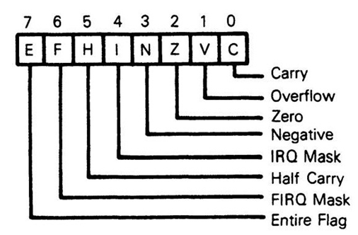
Figure2.1: Condition code registers.
INTERNAL ARCHITECTURE OF MC6800 MICROPROCESSOR:
The MC6800 implemented a complex set computer (CISC) design methodology. It featured sixteen address lines giving a total address space of 64K bytes. The 8-bit data bus is bidirectional as well as three-state, making direct memory addressing and micro processing applications realizable.
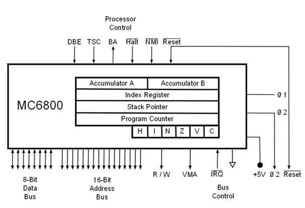
Figure 2.2: Block diagram of MC6800 microprocessor.
The MC6800 microprocessor has 40 pins. According similarities all these pins are divided into five groups:
· Address/data bus.
· Start signal.
· Bus control signals.
· Interrupt signals.
· Direct Memory Access (DMA) signal
MC6809 CLOCKS:
The MC6809 has four pins committed to developing the clock signals needed for internal and system operation. They are: the oscillator pins EXTAL and XTAL; the standard M6800 enable (E) clock; and a new, quadrature (Q) clock.
- Oscillator (EXTAL, XTAL) : These pins are used to connect the processor’s internal oscillator to an external, parallel-resonant crystal. These pins can also be used for input of an external TTL timing signal by grounding the XTAL pin and applying the input to the EXTAL pin. The crystal or the external timing source is four times the resulting bus frequency.
- Enable (E) : The E clock is similar to the phase 2 (ø2) MC6800 bus timing clock. The leading edge indicates to memory and peripherals that the data is stable and to begin write operations. Data movement occurs after the Q clock is high and is latched on the trailing edge of E. Data is valid from the processor (during a write operation) by the rising edge of E.
- Quadrature (Q) : The Q clock leads the E clock by approximately one half of the E clock time. Address information from the processor is valid with the leading edge of the Q clock. The Q clock is a new signal in these processors and does not have an equivalent clock within the MC6800 bus timing.
MC6809E CLOCKS (E and Q):
The MC6809E has two pins provided for the TTL clock signal inputs required for internal operation. They are the standard M6800 enable (E) clock and the quadrature (Q) clock. The Q input must lead the E input.
Addresses will be valid from the processor (on address delay time after the falling edge of E) and data will be latched from the bus by the falling edge of E. The Q input is fully TTL compatible. The E input is used to drive the internal MOS circuitry directly and therefore requires input levels above the normal TTL levels.
THREE STATE CONTROLS (TSC) :
This input is used to place the address and data lines and the R/W line in the high-impedance state and allows the address bus to be shared with other bus masters.
LAST INSTRUCTION CYCLE (LIC):
This output goes high during the last cycle of every instruction and its high-to-low transition indicates that the first byte of an opcode will be latched at the end of the present bus cycle.
ADDRESS BUS (A0-A15):
This 16-bit, unidirectional, three-state bus is used by the processor to provide address information to the address bus. Address information is valid on the rising edge of the Q clock. All 16 outputs are in the high-impedance state when the bus available (BA) signal is high, and for one bus cycle thereafter.
When the processor does not require the address bus for a data transfer, it outputs address FFFF16, and read/write (R/W) high. This is a “dummy access” of the least-significant byte of the reset vector which replaces the valid memory address (VMA) functions of the MC6800. For the MC6809, the memory read signal internal circuitry inhibits stretching of the clocks during non-access cycles.
DATA BUS (D0-D7):
This 8-bit, bidirectional, three-state bus is the general purpose data path. All eight outputs are in the high-impedance state when the bus available (BA) output is high.
READ/WRITE (R/W):
This output indicates the direction of data transfer on the data bus. A low indicates that the processor is writing onto the data bus; a high indicates that the processor is reading data from the data bus. The signal at the R/W output is valid at the leading edge of the Q clock. The R/W output is in the high-impedance state when the bus available (BA) output is high.
RESET (RESET):
This input is used to reset the processor. A low input lasting longer than one bus cycle will reset the processor. The reset vector is fetched from locations $FFFE and $FFFF when the processor enters the reset acknowledge state as indicated by the BA output being low and the BS output being high. During initial power-on, the reset input should be held low until the clock oscillator is fully operational.
PROCESSOR STATE INDICATORS (BA, BS):
The processor uses these two output lines to indicate the present processor state. These pins are valid with the leading edge of the Q clock.
The bus available (BA) output is used to indicate that the buses (address and data) and the read/write output are in the high-impedance state. This signal can be used to indicate to bus-sharing or direct memory access systems that the buses are available. When BA goes low, an additional dead cycle will elapse before the processor regains control of the buses.
The bus status (BS) output is used in conjunction with the BA output to indicate the present state of the processor. Table 1-1 is a listing of the BA and BS outputs and the processor states that they indicate. The following paragraphs briefly explain each processor state.
| |||||||||||||||||
INTERRUPTS:
The processor has three separate interrupt input pins: non-maskable interrupt (NMI), fast interrupt request (FIRQ), and interrupt request (IRQ). These interrupt inputs are latched by the falling edge of every Q clock except during cycle stealing operations where only the NMI input is latched. Using this point as a reference, a delay of at least one bus cycle will occur before the interrupt is recognized by the processor.
MEMORY READ (MRDY):
This input allows extension of the E and Q clocks to allow a longer data access time. A low on this input allows extension of the E and Q clocks (E high and Q low) in integral multiples of quarter bus cycles (up to 10 cycles) to allow interface with slow memory devices. Memory ready does not extend the E and Q clocks during non-valid memory access cycles and therefore the processor does not slow down for “don’t care” bus accesses. Memory ready may also be used to extend the E and Q clocks when an external device is using the halt and direct memory access/bus request inputs.
HALT:
This input is used to halt the processor. A low input halts the processor at the end of the present instruction execution cycle and the processor remains halted indefinitely without loss of data. When the processor is halted, the BA output is high to indicate that the buses are in the high-impedance state and the BS output is also high to indicate that the processor is in the halt/bus grant state.
DIRECT MEMORY ACCESS/BUS REQUEST:
This input is used to suspend program execution and make the buses available for another use such as a direct memory access or a dynamic memory refresh. A low level on this input occurring during the Q clock high time suspends instruction execution at the end of the current cycle. The processor acknowledges acceptance of this input by setting the BA and BS outputs high to signify the bus grant state. The requesting device now has up to 15 bus cycles before the processor retrieves the bus for self-refresh.
Typically, a direct memory access controller will request to use the bus by setting the DMA/BREQ input low when E goes high. When the processor acknowledges this input by setting the BA and BS outputs high, that cycle will be a dead cycle used to transfer bus mastership to the direct memory access controller. False memory access during any dead cycle should be prevented by externally developing a system DMAVMA signal which is low in any cycle when the BA output changes.
BUSY (MC6809E):
This output indicates that bus re-arbitration should be deferred and provides the indivisible memory operation required for a “test-and-set” primitive.
This output will be high for the first two cycles of any Read-Modify-Write instruction, high during the first byte of a double-byte access, and high during the first byte of any indirect access or vector-fetch operation.
POWER:
Two inputs are used to supply power to the processor: VCC is +5.0 ±5%, while VSS is ground or 0 volts.
4
PROCESSOR CYCLE OF MC6800 PROCESSOR
| CHAPTER 4 |
PROCESSOR CYCLE OF MC6800 PROCESSOR
BASIC PROCESSOR CYCLE:
- Use fetch-decode-execute principle.
- Controlled by $1 and $2 clocks:
- Rising edge of $1, instruction address put on address bus,
- Failing edge of $1 ,PC by 1,
- Raising edge of $2, data from selected location put on data bus,
- Failing edge of $2 , instruction code (op-code) decoded in IR.
Example:
Loading AccA with 99,
- A 2-cycle operation.
- Note: op-code for loading AccA(LDAA) = 86,
- Assume this op-code stored at $3000
So,PC=$3000, and data ‘99’ is stored at $3001.
5
INSTRUCTION SET &
ADDRESSING MODE
CHAPTER 5 |
INSTRUCTION SET & ADDRESSING MODE
INSTRUCTION SET:
The MC6800 has a set of 72 different executable source instructions. Included are binary and decimal arithmetic, logical, shift, rotate, load, store, conditional, or unconditional branch, manipulation instructions. Each of the 72 executable instructions of the source language assembles into 1 to 3 bytes of machine code. The number of bytes depends on the particular instruction and on the addressing mode.
The coding of the first bytes corresponding to an executable instruction is sufficient to identify the instruction and addressing mode. There are 197 valid machine codes, 59 of the 256 possible codes being unassigned.
When an instruction translates into two or three bytes of code, the second byte, or the second and third byte contain an operand, an address, or information from which an address is obtained during execution.
Microprocessor instructions are often divided into three general classifications: (1) Memory reference, so called because they operate on specific memory locations; (2) Operating instructions that function without needing a memory reference; (3) I/O instructions for transferring data between the microprocessor and peripheral devices.
In many instances, the MC6800 performs the same operation on both its internal accumulators and the external memory locations. In addition the MC6800 interface adapters (PIA and ACIA) allow the MPU to treat peripheral devices exactly like other memory location, hence no I/O instruction as such are required. Because of this features other classification are more suitable for introducing the MC6800’s instruction set. 1. Accumulator and memory operations. 2. Program control operation. 3. Condition Code register operation.
ADDERESSING MODE:
The addressing modes available on the MC6809 and MC6809E are: Inherent, Immediate, Extended, Direct, Indexed (with various offsets and auto incrementing/decrementing), and Branch Relative. Some of these addressing modes require an additional byte after the opcode to provide additional addressing interpretation. This byte is called a postbyte.The following paragraphs provide a description of each addressing mode. In these descriptions the term effective address is used to indicate the address in memory from which the argument for an instruction is fetched or stored, or from which instruction processing is to proceed.
INHERENT:
The information necessary to execute the instruction is contained in the opcode. Some operations specifying only the index registers or the accumulators, and no other arguments, are also included in this addressing mode.
Example: MUL.
IMMEDIATE:
The operand is contained in one or two bytes immediately following the opcode. This addressing mode is used to provide constant data values that do not change during program execution. Both 8-bit and 16-bit operands are used depending on the size of the argument specified in the opcode.
Another form of immediate addressing uses a post byte to determine the registers to be manipulated. The exchange (EXG) and transfer (TFR) instructions use the post byte as shown in Figure 5-1(A). The push and pull instructions use the post byte to designate the registers to be pushed or pulled as shown in Figure 5-1(B).
| ||||||||||||||||||||||||||||||||||||||||||||||||||||||||||||
| ||||||||||||||||||||||||||||||||||||||||||||||||||||||||||||
| ||||||||||||||||||||||||||||||||||||||||||||||||||||||||||||
Figure 2-1: Post byte Usage for EXG/TFR, PSH/PUL Instructions.
EXTENDED:
The effective address of the argument is contained in the two bytes following the opcode. Instructions using the extended addressing mode can reference arguments anywhere in the 64K addressing space. Extended addressing is generally not used in position independent programs because it supplies an absolute address. Example: LDA>CAT.
DIRECT:
The effective address is developed by concatenation of the contents of the direct page register with the byte immediately following the opcode. The direct page register contents are the most-significant byte of the address. This allows accessing 256 locations within any one of 256 pages. Therefore, the entire addressing range is available for access using a single two-byte instruction.
Example :LDA >CAT.
INDEXED:
In these addressing modes, one of the pointer registers (X, Y, U, or S), and sometimes the program counter (PC) is used in the calculation of the effective address of the instruction operand. The basic types (and their variations) of indexed addressing available are shown in Table 2-1 along with the postbyte configuration used.
BRANCH RELATIVE:
This addressing mode is used when branches from the current instruction location to some other location relative to the current program counter are desired. If the test condition of the branch instruction is true, then the effective address is calculated (program counter plus twos complement offset) and the branch is taken. If the test condition is false, the processor proceeds to the next in-line instruction. Note that the program counter is always pointing to the next instruction when the offset is added. Branch relative addressing is always used in position independent programs for all control transfers.
For short branches, the byte following the branch instruction opcode is treated as an 8-bit signed offset to be used to calculate the effective address of the next instruction if the branch is taken. This is called a short relative branch and the range is limited to plus 127 or minus 128 bytes from the following opcode.
For long branches, the two bytes after the opcode are used to calculate the effective address. This is called a long relative branch and the range is plus 32,767 or minus 32,768 bytes from the following opcode or the full 64K address space of memory that the processor can address at one time.
| Examples: | Short Branch | Long Branch |
| BRA POLE | LBRA CAT |
6
PROGRAMING
MODEL
| CHAPTER 6 |
PROGRAMING MODEL
| ||||||||
| ||||||||
| ||||||||
| ||||||||
|
A – Accumulator A
B – Accumulator B
X – Index register
PC – Program Counter
SP – Stack Pointer
CCR – Conditional Code Register: Half carry, Interrupt mask, Negative, Zero, overflow and Carry
The 6800 is a standard “8-bit” 2’s complement microprocessor, like the Intel 8080. It supports 8-bit bytes, 16-bit addresses and 64 KB of memory. Like the 8080, code can be placed in ROM. This is an important feature compared to some of the minicomputers of the time, especially the PDP-8, which used a linked-list embedded in the code for subroutine linkage.
The 6800 had a 16-bit stack pointer, so the stack can be located anywhere and can grow to any length up to the size of the memory. Compare this with the 6502 which had only an 8-bit stack pointer and which mapped the stack into the second page (addresses 256 – 511).
Like the 8080, the 6800 supports multi-precision arithmetic using a carry flag and the ADC (add with carry) and SBC (subtract with carry) instructions. Decimal arithmetic is supported in a fashion similar to the 8080: there is a DAA (decimal adjust accumulator) instruction, which corrects the result of the 2’s complement ADD on two packed decimal digits. Unlike the 6502, the 6800 also provided add and subtract without carry (ADD and SUB instructions).
Arithmetic instructions set the usual 2’s complement flags: Sign, Zero, oVerflow and Carry. Unlike the 8080 and the 6502, the 6800 had a complete set of branch instructions, basically identical to those provided on the PDP-11, for comparing both signed and unsigned quantities. For example, if you want to compare i with j, then load i into an accumulator (LDAA i), compare or subtract with j (CMPA j or SUBA j) and then branch:
- BEQ – Branch if i equals j
- BNE – Branch if i does not equal j
- BHI – Branch if i is greater than j (unsigned)
- BHS – Branch if i is higher or same as j (unsigned)
- BLO – Branch if i is lower than j (unsigned)
- BLS – Branch if i is lower than or equal to j (unsigned)
- BGT – Branch if i is greater than j (signed)
- BGE – Branch if i is greater than or equal to j (signed)
- BLT – Branch if i is less than j (signed)
- BLE – Branch if i is less than or equal to j (signed)
- BPL – Branch if plus (positive or zero)
- BMI – Branch if minus (negative)
- BCC – Branch if Carry clear (same as BHS)
- BCS – Branch if Carry set (same as BLO)
- BVS – Branch if overflow set
- BVC – Branch if overflow clear
- BRA – Branch always
| CRITICISMS |
There are a number of problems which were remedied in later devices, such as the 6809 and 6811:
- Only one pointer register. Although the stack pointer can be used in tight copy loops, it is awkward and interrupts have to be disabled for this trick. The 6800’s most important competitor, the 8080, had three pointers (but no indexing).
- Stack instructions use post-decrement on push and pre-increment on pop instead of the more natural post-increment on pop and pre-decrement on push (SP pointing at the top element). This shows up when the stack pointer is transferred to the index register: the first thing on the stack is at offset 1.
- The index register cannot be directly pushed or popped from the stack.
- The accumulators and index registers occupy different spaces and thus there are no instructions to transfer or operate between the two. For example, there is no way to directly add an accumulator or even a constant to the index register. Later processors remedied this by adding the “ABX” (add B to X) and “LEA” (load effective address) instructions.
- The CPX (compare X) instruction does not affect the Carry flag, so direct magnitude comparisons with the index register are not possible.
- The DAA (decimal adjust) instruction only worked after addition, and not subtraction. To subtract packed decimal, one had to use 9’s complement followed by addition. Other microprocessors solved this problem in various ways: The 6502 had a decimal mode bit: when set both the normal addition and subtraction instructions operated on packed decimal. The Z80 had a subtraction bit in its status flags. If the last operation was a subtraction, this bit was set to let the decimal adjust instruction know to operate differently. The 8086 simply had a DAS (decimal adjust for subtraction) instruction.
DESIGNERS |
It’s not clear if there was a chief architect, but the two main designers were Chuck Peddle and Charles Melear. Some of the 6800 designers went on to join MOS Technology where they created the 6502. These included Chuck Peddle and Bill Mensch.
Charles Melear continued working at Motorola on the 6800 family and the 683xx family including the 68332.
Bill Mensch designed the MC6820 PIA (Peripheral Interface Adapter).
REFERENCES |
- Motorola (1976), Motorola Annual Report 1975, pp. 13 “We introduced our M6800 microprocessor system late in 1974 and it gained broad industry acceptance in 1975.”
- Microprocessor Report, Volume 10, Number 10, August 5, 1996
- Ken Polsson, Chronology of Events in the History of Microcomputers – 1971-1976 The Birth of the Microcomputer “Motorola introduces its 6800 chip, an early 8-bit microprocessor used in microcomputers and industrial and automotive control devices. The 6800 was designed by Chuck Peddle and Charlie Melear.”
- The Freeman PC Museum, PC Timeline.
- http://en.wikipedia.org/wiki/Motorola_6800
- www.google.com
- www.maddes.net/m6809pm/sections.htm