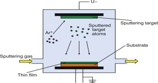
Physical Vapor Deposition (PVD) is a thin film deposition technique used in materials science and engineering to deposit thin films of various materials onto a substrate. PVD involves the physical transport of atoms or molecules from a source material (the target) to the substrate by vaporization, which occurs under vacuum conditions. The vaporized atoms or molecules then condense on the substrate, forming a thin film.
PVD, also known as physical vapor transport (PVT), refers to a class of vacuum deposition methods that can be used to create thin films and coatings on substrates such as metals, ceramics, glass, and polymers. PVD is defined by the material transitioning from a condensed phase to a vapor phase and then back to a thin film condensed phase. Sputtering and evaporation are the two most common PVD processes.
There are several techniques for PVD, including thermal evaporation, sputtering, and ion plating. In thermal evaporation, the material is heated until it evaporates and condenses onto the substrate. Sputtering involves bombarding a target material with high-energy particles to release atoms, which then deposit onto the substrate. Ion plating uses a combination of thermal evaporation and ion bombardment to produce a high-quality film.
There are several techniques used in PVD, including:
- Thermal evaporation: In this technique, the target material is heated to a high temperature, causing it to vaporize and condense on the substrate.
- Sputtering: In this technique, a plasma is used to bombard the target material, causing atoms or molecules to be ejected from the target and deposited on the substrate.
- Electron beam evaporation: In this technique, an electron beam is used to heat the target material, causing it to vaporize and condense on the substrate.
- Ion plating: In this technique, ions of the target material are accelerated towards the substrate, causing them to deposit and form a thin film.
Application
PVD is widely used in many applications, including the semiconductor industry, the manufacture of hard coatings, and the production of optical coatings for lenses and mirrors.
PVD is used to make items that require thin films for optical, mechanical, electrical, acoustic, or chemical functions. Thin-film solar cells are an example of a semiconductor device, as are microelectromechanical devices such as a thin-film bulk acoustic resonator, aluminized PET film for food packaging and balloons, and titanium nitride-coated cutting tools for metalworking. Aside from PVD fabrication tools, special smaller tools primarily used for scientific purposes have been developed.
Most other surfaces inside the vacuum chamber, including the fixturing used to hold the parts, are unavoidably deposited with the source material. This is known as overshoot.