Microscopy images are images captured using a microscope. These can provide detailed information about the structure, composition, and properties of microscopic samples, such as cells, tissues, bacteria, viruses, and other small organisms.
Excitons are drawing attention as possible quantum bits (qubits) in tomorrow’s quantum computers and are central to optoelectronics and energy-harvesting processes. Although they can be found in semiconductors and other materials, these charge-neutral quasiparticles are notoriously challenging to contain and control.
Researchers have now produced and directly observed extremely localized excitons that are contained in straightforward stacks of atomically thin materials for the first time. The research supports theoretical hypotheses and opens up new possibilities for using specially designed materials to control excitons.
“The idea that you can localize excitons on specific lattice sites by simply stacking these 2D materials is exciting because it has a variety of applications, from designer optoelectronic devices to materials for quantum information science,” said Archana Raja, co-lead of the project and a staff scientist at Lawrence Berkeley National Laboratory’s (Berkeley Lab) Molecular Foundry, whose group led the device fabrication and optical spectroscopy characterization.
We used basically all the most advanced capabilities on our most advanced microscope to do this experiment. We were pushing the boundaries of everything we can do, from making the sample to analyzing the sample to doing the theory.
Peter Ercius
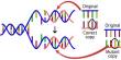
By stacking layers of tungsten diselenide (WS2) and tungsten disulfide (WSe2), the researchers created devices. A moiré superlattice, a bigger periodic pattern that results from the overlap of two smaller patterns with similar but different elemental spacing, was created as a result of a little difference in the atom spacing between the two materials.
The researchers gathered structural and spectroscopic data on the devices using cutting-edge electron microscopy equipment, combining data from hundreds of experiments to identify the likely locations of excitons.
“We used basically all the most advanced capabilities on our most advanced microscope to do this experiment,” said Peter Ercius, who led the imaging work at the Molecular Foundry’s National Center for Electron Microscopy. “We were pushing the boundaries of everything we can do, from making the sample to analyzing the sample to doing the theory.”
Large atomic reconstructions occur in the stacked materials, modulating the electronic structure to create a periodic array of “traps” where excitons become localized, according to theoretical calculations led by Steven Louie, a distinguished professor of physics at UC Berkeley and faculty senior scientist at Berkeley Lab.
A novel method for creating optoelectronic materials has been established as a result of the discovery of this direct connection between structural modifications and the localisation of excitons.
The team’s findings are described in a paper published in the journal Science with postdoctoral fellows Sandhya Susarla (now a professor at Arizona State University) and Mit H. Naik as co-lead authors. Next, the team will examine techniques to adjusting the moiré lattice on demand and make the phenomena more resilient to material disorder.