Scientists at the Department of Energy’s Oak Ridge National Laboratory used an electron microscope to precisely create tiny electrically conductive cubes that can interact with light and organize them in patterned patterns that limit and relay light’s electromagnetic signal.
This demonstration could pave the way for quicker computer chips and more perceptive sensors in the future. The capacity of these structures’ surfaces to support collective waves of electrons, known as plasmons, with the same frequency as light waves but considerably tighter confinement, gives them the appearance of sorcery.
The light-guiding structures are measured in nanometers, which is 100,000 times smaller than human hair.
“These nanoscale cube systems allow extreme confinement of light in specific locations and tunable control of its energy,” said ORNL’s Kevin Roccapriore, first author of a study published in the journal Small. “It’s a way to connect signals with very different length scales.”
This achievement could be crucial for quantum and photonic computing. Quantum computers use quantum bits, or qubits, that are determined by a particle’s quantum state, such as its spin. In comparison to a single value saved by a traditional bit, qubits can hold multiple values.
In optical computers, light electromagnetic radiation propagated by massless fundamental particles called photons replaces electrons as the carrier. Because photons travel faster than electrons and do not emit heat, optical computers could outperform traditional computers in terms of performance and energy efficiency.
Future technologies may use the best of both worlds.
“Light is the preferred way to communicate with qubits, but you cannot connect contacts to them directly,” said senior author Sergei Kalinin of ORNL. “The problem with visible light is its wavelengths range from about 380 nanometers for violet to around 700 nanometers for red. That’s too big because we want to make devices only a few nanometers in size. This work aims to create a framework to move technology beyond Moore’s law and classical electronics. If you try to put ‘light’ and ‘small’ together, that’s exactly where plasmonics comes into play.”
Electron energy loss spectroscopy provides deep insights into exotic physics and quantum phenomena related to plasmonic behavior. Electron energy loss spectroscopy lets us analyze evolving plasmonic responses in real-time as the cubes are sculpted. We can figure out relationships between arrangements of cubes and their plasmonic properties.
Andrew Lupini
If plasmonics has a bright future, the ORNL-led achievement could help overcome a signal size mismatch that concerns the integration of components composed of various materials. In next-generation optoelectronic devices, such hybrid components will need to “talk” to each other. Plasmonics may be able to fill the void.
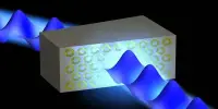
Metals, which are conductive because to their free electrons, were the first to exhibit plasmonic phenomena. The ORNL researchers employed cubes constructed of indium oxide doped with tin and fluorine, a transparent semiconductor that behaves like a metal.
The cube’s energy tunability is due to the fact that it is a semiconductor. A light wave’s energy is proportional to its frequency. The shorter the wavelength, the higher the frequency. The human eye perceives visible light wavelengths as colors.
Because a semiconductor may be doped, or have a little impurity introduced to it, the wavelength of the semiconductor can be changed on the spectrum. The cubes in the study were each 10 nanometers broad, which is far smaller than the visible light wavelength.
The cubes were created by Shin-Hum Cho and Delia Milliron at the University of Texas at Austin and were immersed in a detergent to prevent clumping before being pipetted onto a substrate, where they self-assembled into a two-dimensional array.
Each cube was enveloped by a layer of detergent, equally spacing them apart. The arrays were shipped to ORNL after the detergent was removed.
“That the cubes do not directly touch is important for the collective behavior,” said Roccapriore, who organized the cubes into diverse structures. “Each cube individually has its own plasmon behavior. When we bring them together in geometries like a nanowire, they talk to one another and produce new effects that are not typically seen in similar geometries that aren’t made up of individual elements.”
The research expands on previous work using an electron beam to shape three-dimensional structures as small as a nanometer.
“The current paper proves that the plasmonic effect, as well as the structure, can be sculpted,” Roccapriore said. “At the end of the day, we’re interested in the electron wave where is it, and what is its energy? We’re controlling those two things.”
Kalinin added, “We want to transition from using what exists in nature by chance to fabricating materials with the right responses. We can take a system of cubes, shine a light on it and channel energy into small volumes localized exactly where we want them to be.”
Roccapriore had done a lot of electron-beam lithography in graduate school and even built a machine in his garage to produce and mill 3D-printed structures, so the project was a natural fit for him.
He experimented with the current of an electron microscope’s beam at ORNL, shifting it from imaging to modification mode on purpose. He discovered that he could remove individual cubes or complete cubes from an array at any time to create patterned things. He also discovered that just as adding chemical components to cube energies allows them to be tuned, selectively removing chemical elements allows them to be tuned as well.
Scanning transmission electron microscopy, or STEM, allows for such atomic precision. A technique termed electron energy loss spectroscopy proved crucial in understanding plasmonic activity within single cubes and among collective cube assemblies.
It makes use of a STEM device with an electron beam filtered to a certain range of energies. The electrons in the beam lose energy as they move through the sample, interact with electrons in the material, and then transmit a small amount of energy to the system via activating plasmons.
“Electron energy loss spectroscopy provides deep insights into exotic physics and quantum phenomena related to plasmonic behavior,” said co-author Andrew Lupini of ORNL, who helped map the energies of electrons in the cubes and arrays of cubes. Lupini is one of the developers of aberration-corrected STEM, which made pioneering advances possible.
“Electron energy loss spectroscopy lets us analyze evolving plasmonic responses in real-time as the cubes are sculpted. We can figure out relationships between arrangements of cubes and their plasmonic properties.”
The researchers want to build a database of material, structural, and plasmonic characteristics correlations. This new information will provide the groundwork for mass-producing structures that can direct the passage of light in plasmonic nanocircuits in the future.
According to Roccapriore, “the idea is to understand the relationships using machine learning and then automate the process.”