Raman imaging is a powerful technique that can provide detailed chemical information about a sample at the nanoscale. It is particularly useful for studying samples that are too large or complex for traditional techniques such as transmission electron microscopy. One of the challenges in using Raman imaging for large samples is maintaining stable, sustained imaging over a long period of time.
Raman spectroscopy, an optical microscopy technique, provides extensive molecular fingerprint information regarding chemical structure, phase, crystallinity, and molecular interactions. It is a non-destructive chemical analysis technique. The process depends on how light interacts with chemical interactions in a material.
Optical microscopes, however, are unable to discern distances that are less than half the wavelength of the light impinge on the sample since light is a wave. The “diffraction limit” is what precludes optical microscopy methods like Raman spectroscopy from resolving objects at the nanoscale.
Another method known as “tip-enhanced Raman spectroscopy (TERS),” which can achieve spatial resolutions below the diffraction limit, was developed to increase the spatial resolution.
In TERS, a metallic tip that is only a few nanometers in size limits the light to a small space just above the sample. The light interacts with the sample molecules on the surface, and by examining the scattered light, imaging is accomplished.
Chemical compositions and surface flaws in samples have been effectively analyzed at nanoscale resolutions using TERS. However, due to inherent thermal and vibrational oscillations in ambient circumstances, the nanotip tends to drift during imaging, leading to either sample out-of-focus, misalignment between the nanotip and focal region, or both. The scattered signals are significantly distorted as a result.
This limits imaging of any sample larger than 1 µm2 with nanoscale resolution since TERS imaging needs to be finished within a time window of 30 minutes.
Our new drift-compensated TERS microscopy could not only evaluate surface properties of device materials better but also allow us to study biological processes such as the mechanism underlying the development of diseases. This, in turn, could help develop novel clinical methods and therapies.
Dr. Takayuki Umakoshi
In a new study published in Science Advances, a research team from Japan, led by Dr. Ryo Kato, a designated Assistant Professor at the Institute of Post-LED Photonics at Tokushima University, and Associate Professor Takayuki Umakoshi and Professor Prabhat Verma from Osaka University, has now developed, for the first time, a stable TERS system that is not limited to a short imaging time window.
The group successfully imaged nanoscale flaws over a 6-hour period in a micrometer-sized, two-dimensional (2D) tungsten disulfide (WS2) film, a material frequently utilized in optoelectronic devices, as a demonstration of its capabilities..
“Our new optical nano-imaging system enables characterization of defect analysis in large-sized WS2 layers at a high pixel resolution down to 10 nm without any significant loss of optical signal,” says Dr. Kato.
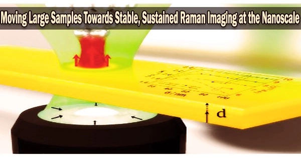
The team created a feedback system that tracks the movement of the focused light source and repositions the focus plane as necessary to account for drifts over extended durations.
The displacement of a reflected laser guide beam that is pointed into the microscope is used to track where the light source’s focal point is located. A piezo-controlled objective scanner is then used to stabilize the focus whenever the system detects a drift or change in the light source’s focal point.
The researchers created a tip drift adjustment mechanism helped by laser scanning to steady the nanotip. In this instance, as the metallic nanotip approaches the sample surface, galvano-scanners capture photos of the laser spot surrounding it. The location of the nanotip is seen in this image as a bright point.
After performing the measurement at a specific pixel, a new image of the laser spot surrounding the nanotip is taken. The nanotip is then shifted in this image to correspond with the new location of the laser spot. The procedure is carried out repeatedly to maintain the nanotip’s location during the imaging procedure.
By implementing these corrections, the team was able to image a 2D sheet of WS2 with a scan area of 1 × 4 µm2. They were able to find special problems that normal TER imaging missed by using an imaging time window that was 12 times larger.
Additionally, they demonstrated that the defect density was higher on a larger WS2 sample (equivalent to device scales) than had been previously reported for smaller samples. The research may pave the way for exact, high-resolution imaging of biological samples as well as optoelectronic components.
“Our new drift-compensated TERS microscopy could not only evaluate surface properties of device materials better but also allow us to study biological processes such as the mechanism underlying the development of diseases. This, in turn, could help develop novel clinical methods and therapies,” speculates Dr. Umakoshi. These are certainly some exciting possibilities to contemplate!