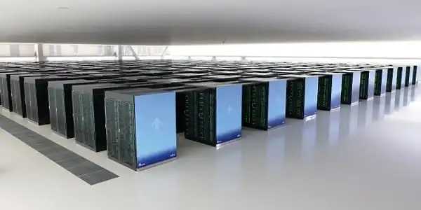
Any of a class of extraordinarily powerful computers is referred to as a supercomputer. The word is widely used to refer to the most powerful high-performance systems available at any particular moment. Such computers have mostly been utilized for scientific and engineering activity that necessitates extremely fast computations.
An examination of the process of extending ‘Moore’s law,’ which has roughly doubled the number of transistors that can be packed on a microchip every two years, and developing new ways to build more powerful, efficient, and cost-effective processors.
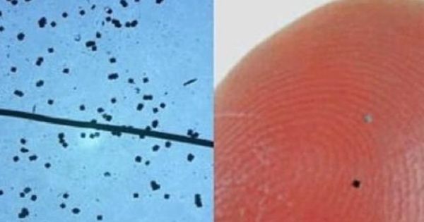
Over the course of nearly 60 years, the information age has given the world the internet, smartphones, and lightning-fast computers. This has been made possible by the roughly two-year-long doubling of the number of transistors that can be packed onto a computer chip, resulting in billions of atomic-scale transistors that now fit on a fingernail-sized device. Individual atoms can be observed and counted in these “atomic-scale” lengths.
As a first step, the simulations largely agreed with the results and could lead to a better understanding of the application of ALE for atomic-scale etching. It all starts with increasing our fundamental understanding of atomic layer etching.
Joseph Vella
Physical limit
With this doubling approaching a physical limit, the United States Department of Energy’s (DOE) Princeton Plasma Physics Laboratory (PPPL) has joined industry efforts to prolong the process and discover new techniques to make ever-more competent, efficient, and cost-effective chips. In the first PPPL study under a Cooperative Research and Development Agreement (CRADA) with Lam Research Corp., a global producer of chip-making equipment, laboratory scientists properly predicted a fundamental stage in atomic-scale chip creation using modeling.
“This would be one small piece in the overall process,” said David Graves, associate laboratory director for low-temperature plasma surface interactions, professor in the Princeton Department of Chemical and Biological Engineering, and co-author of a paper describing the findings published in the Journal of Vacuum Science & Technology B. Insights gleaned through modeling, he said, “may lead to all sorts of positive things, and that’s why this endeavor at the Lab has some promise.”
While the shrinkage can’t last much longer, “it hasn’t fully stopped,” he says. “To date, industry has been successful in developing innovative new processes primarily through empirical approaches, but a better fundamental knowledge will accelerate this process. Fundamental research demand time and skill that the industry does not always have” He stated.
The PPPL researchers modeled “atomic layer etching” (ALE), a fundamental fabrication step that aims to remove single atomic layers from a surface at a time. This method may be used to etch intricate three-dimensional structures into a coating on a silicon wafer with crucial dimensions hundreds of times thinner than a human hair.

Basic agreement
“As a first step, the simulations largely agreed with the results and could lead to a better understanding of the application of ALE for atomic-scale etching,” said Joseph Vella, a postdoctoral scholar at PPPL and main author of the journal publication. “It all starts with increasing our fundamental understanding of atomic layer etching,” he said, adding that improved understanding will allow PPPL to explore things like the level of surface damage and the degree of roughness created during ALE.
On an atomic scale, the model mimicked the sequential employment of chlorine gas and argon plasma ions to manage the silicon etch process. Plasma, also known as ionized plasma, is a gas composed of free electrons, positively charged ions, and neutral molecules. In contrast to the ultra-hot plasma utilized in fusion research, the plasma used in semiconductor device production is around room temperature.
“A surprising empirical discovery from Lam Research was that the ALE method became more efficient when the ion energies were quite a bit greater than the ones we started with,” Graves explained. “So our next step in the simulations will be to see if we can understand what happens when the ion energy is significantly higher and why it’s so excellent.”
In the future, “the semiconductor industry as a whole is envisioning a significant expansion in the materials and types of devices to be employed, and this expansion will also require atomic-scale precision,” he said. “The United States’ mission is to lead the world in using research to solve critical industrial challenges,” he explained, “and our work is part of that.”
Chips are meant to get smaller and more powerful in the computer industry – but one company, Cerebras Systems, has turned that paradigm on its head and is instead manufacturing tremendously powerful computer chips the size of dinner plates that can outperform even supercomputers. And now, the world’s largest AI chip has more than doubled its specifications — without adding a single inch to its size.


