In wastewater treatment, graphene and graphene oxide-based structures have promising applications for the removal of toxic contaminants such as heavy metals, synthetic dyes, pharmaceuticals, and microorganisms. Graphene-based structures demonstrated superior adsorption capacities in the presence of the aforementioned contaminants.
Researchers created a new graphene-based nanoelectronics platform that is compatible with traditional microelectronics manufacturing, paving the way for silicon’s replacement. The search for a material that can replace silicon is a pressing issue in the field of nanoelectronics.
For decades, graphene has appeared to be promising. However, its potential was stifled along the way due to harmful processing methods and a lack of a new electronics paradigm to embrace it. With silicon’s ability to support faster computing nearly exhausted, the next big nanoelectronics platform is needed now more than ever.
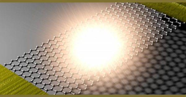
Walter de Heer, Regents’ Professor in the School of Physics at Georgia Institute of Technology, has taken an important step forward in making the case for silicon’s replacement. De Heer and colleagues created a new nanoelectronics platform based on graphene, which is a single sheet of carbon atoms. The technology is compatible with standard microelectronics manufacturing, which is a requirement for any viable alternative to silicon. The team may have discovered a new quasiparticle during their research, which was published in Nature Communications. Their discovery has the potential to lead to the production of smaller, faster, more efficient, and more sustainable computer chips, as well as implications for quantum and high-performance computing.
Quantum interference has been observed in carbon nanotubes at low temperatures, and we expect to see similar effects in epigraphene ribbons and networks. This important feature of graphene is not possible with silicon.
de Heer
“Graphene’s power lies in its flat, two-dimensional structure that is held together by the strongest chemical bonds known,” de Heer said. “It was clear from the beginning that graphene can be miniaturized to a far greater extent than silicon – enabling much smaller devices while operating at higher speeds and producing much less heat. This means that, in principle, more devices can be packed on a single chip of graphene than with silicon.”
In 2001, de Heer proposed an alternative form of electronics based on epitaxial graphene, or epigraphene – a layer of graphene that was found to spontaneously form on top of silicon carbide crystal, a semiconductor used in high-power electronics. At the time, researchers found that electric currents flow without resistance along epigraphene’s edges, and that graphene devices could be seamlessly interconnected without metal wires. This combination allows for a form of electronics that relies on the unique light-like properties of graphene electrons.
“Quantum interference has been observed in carbon nanotubes at low temperatures, and we expect to see similar effects in epigraphene ribbons and networks,” de Heer said. “This important feature of graphene is not possible with silicon.”
Creating the Platform
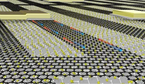
The researchers used a modified form of epigraphene on a silicon carbide crystal substrate to create the new nanoelectronics platform. They created unique silicon carbide chips from electronics-grade silicon carbide crystals in collaboration with researchers at the Tianjin International Center for Nanoparticles and Nanosystems at the University of Tianjin, China. Graphene was grown in de Heer’s Georgia Tech laboratory using patented furnaces.
The researchers carved the graphene nanostructures and welded their edges to the silicon carbide chips using electron beam lithography, a technique commonly used in microelectronics. This process mechanically stabilizes and seals the edges of graphene, which would otherwise react with oxygen and other gases, interfering with the motion of the charges along the edge.
Finally, to measure the electronic properties of their graphene platform, the team used a cryogenic apparatus that allows them to record its properties from a near-zero temperature to room temperature.
Observing the Edge State
The electric charges the team observed in the graphene edge state were similar to photons in an optical fiber that can travel over large distances without scattering. They found that the charges traveled for tens of thousands of nanometers along the edge before scattering. Graphene electrons in previous technologies could only travel about 10 nanometers before bumping into small imperfections and scattering in different directions.
“What’s special about the electric charges in the edges is that they stay on the edge and keep on going at the same speed, even if the edges are not perfectly straight,” said Claire Berger, a physics professor at Georgia Tech and director of research at the French National Center for Scientific Research in Grenoble, France.
In metals, electric currents are carried by negatively charged electrons. But contrary to the researchers’ expectations, their measurements suggested that the edge currents were not carried by electrons or by holes (a term for positive quasiparticles indicating the absence of an electron). Rather, the currents were carried by a highly unusual quasiparticle that has no charge and no energy and yet moves without resistance. The components of the hybrid quasiparticle were observed to travel on opposite sides of the graphene’s edges, despite being a single object.
The unique properties indicate that the quasiparticle might be one that physicists have been hoping to exploit for decades – the elusive Majorana fermion predicted by Italian theoretical physicist Ettore Majorana in 1937.
“Developing electronics using this new quasiparticle in seamlessly interconnected graphene networks is game-changing,” de Heer said. It will likely be another five to 10 years before we have the first graphene-based electronics, according to de Heer. But thanks to the team’s new epitaxial graphene platform, technology is closer than ever to crowning graphene as a successor to silicon.