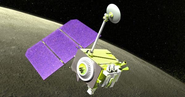
NASA’s Orion spacecraft, which will send men to Mars, is pushing the boundaries of human exploration. However, spacecrafts are exposed to a constant stream of harmful cosmic radiation during their transit, which can impair or even kill onboard equipment.
Researchers report in ACS Nano that carbon nanotube transistors and circuits may be programmed to keep their electrical properties and memory after being attacked by large amounts of radiation, which could help extend future missions.
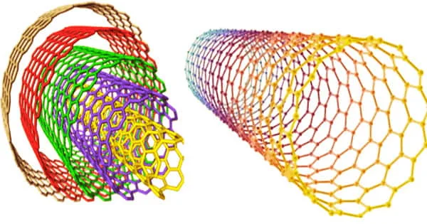
Carbon nanotubes (CNTs) are cylinder-shaped molecules made up of rolled-up single-layer carbon atom sheets (graphene). Carbon nanotubes with a single wall (SWCNTs) Single-wall carbon nanotubes, with diameters in the nanometer range, are an allotrope of carbon midway between fullerene cages and flat graphene.
Deep space missions’ longevity and range are currently constrained by the energy efficiency and robustness of the technology that powers them. Harsh radiation in space, for example, can damage electronics and produce data errors, or even lead computers to crash totally.
Tubes with an unknown carbon-wall structure and diameters smaller than 100 nanometers are also referred to as carbon nanotubes. CNTs are chemically connected with sp2 bonds, an extraordinarily powerful form of molecular contact, just like its building block graphene (why not read our thorough tutorial on graphene, which includes a beautiful infographic).
Carbon nanotubes could be employed in commonly used electronic components like field-effect transistors, for example. Compared to standard silicon-based transistors, these single-atom-thick tubes are projected to make transistors more energy efficient.
While some carbon nanotubes are electrically conductive, others are semiconductors. Because of their nanostructure and the strength of the connections between carbon atoms, they exhibit outstanding tensile strength and thermal conductivity.
In theory, the nanotubes’ ultra-small size should also aid to decrease the effects of radiation striking memory chips containing these materials. However, there hasn’t been much research on the radiation endurance of carbon nanotube field-effect transistors.
As a result, Pritpal Kanhaiya, Max Shulaker, and their colleagues sought to investigate if they could develop this type of field-effect transistor to resist high levels of radiation and use it to build memory chips.
The researchers achieved this by depositing carbon nanotubes as the semiconducting layer in field-effect transistors on a silicon wafer.
Then they evaluated alternative transistor topologies with different levels of shielding surrounding the semiconducting layer, which consisted of tiny layers of hafnium oxide, titanium, and platinum metal.
The researchers discovered that shields above and below the carbon nanotubes preserved the transistor’s electrical properties from incoming radiation up to 10 Mrad, which is far more than most silicon-based radiation-tolerant circuits can manage.
The carbon nanotubes were protected up to 2 Mrad when merely a shield was placed beneath them, which is comparable to commercial silicon-based radiation-tolerant devices.
Finally, the researchers created static random-access memory (SRAM) devices using the bottom shield version of field-effect transistors to achieve a compromise between production simplicity and radiation robustness.
These memory chips have a similar X-ray radiation threshold to silicon-based SRAM devices, just as they did in transistor studies. According to the researchers, these findings suggest that carbon nanotube field-effect transistors, particularly double-shielded versions, could be a promising addition to next-generation electronics for space exploration.