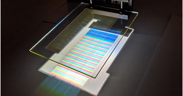
Atomic layer deposition (ALD) is a technique used in materials science to deposit thin films of a material onto a substrate, typically at the nanoscale level. ALD is a type of chemical vapor deposition (CVD) that utilizes a self-limiting surface reaction mechanism to achieve precise control over the thickness and composition of the deposited film.
ALD is a thin-film deposition technique based on the sequential use of a gas-phase chemical process; it is a subclass of chemical vapour deposition. The majority of ALD reactions make use of two chemicals known as precursors (also called “reactants”). These precursors react with the surface of a material one at a time in a sequential, self-limiting manner. Through repeated exposure to separate precursors, a thin film is slowly deposited. ALD is a critical process in the fabrication of semiconductor devices and one of the tools used in the synthesis of nanomaterials.
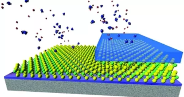
In ALD, a substrate is exposed to alternating pulses of two or more precursor chemicals, typically in a vacuum chamber. Each precursor pulse reacts with the substrate surface in a self-limiting way, depositing a monolayer of material that is only one or a few atoms thick. The substrate is then purged with an inert gas to remove any unreacted precursor molecules before the next precursor pulse is introduced. This process is repeated until the desired film thickness is achieved.
Advantages
ALD offers several advantages over other deposition techniques, including high precision and control over film thickness and composition, conformal coating of complex and high aspect ratio structures, and the ability to deposit materials with high purity and uniformity. It has numerous applications in fields such as microelectronics, catalysis, energy storage, and biomedical engineering.
ALD is a highly controlled method for producing a film with an atomically specified thickness. Furthermore, the formation of various multilayer structures is simple. Because of the equipment’s sensitivity and precision, it is very useful to those working in the fields of microelectronics and nanotechnology in producing small but efficient semiconductors.
Disadvantages
The purity of the substrates is critical, and as a result, the costs will be high. Although this cost may be minor in comparison to the cost of the necessary equipment, it is possible that several trials will be required before finding conditions that favor the desired product. Once the layer has been created and the process has been completed, it may be necessary to remove excess precursors from the final product.
Applications
Atomic layer deposition (ALD) is a thin film deposition technique used in various applications in the semiconductor, solar cell, and energy storage industries. ALD is a process that involves the deposition of thin films, one atomic layer at a time, onto a substrate. The process is controlled by a series of self-limiting chemical reactions between gas-phase precursors and the substrate surface. Here are some common applications of ALD:
- Semiconductors: ALD is used to deposit thin films of semiconducting materials, such as silicon, germanium, and metal oxides, onto semiconductor substrates. These films are used in the fabrication of transistors, capacitors, and other electronic devices.
- Solar cells: ALD is used to deposit thin films of materials, such as metal oxides, onto the surfaces of solar cells. These films act as protective layers, enhance light absorption, and increase the efficiency of the solar cells.
- Catalysis: ALD is used to deposit thin films of catalytic materials onto substrates, such as carbon nanotubes and porous materials. These films improve the catalytic activity of the materials and increase their surface area.
- Gas sensors: ALD is used to deposit thin films of materials onto the surfaces of gas sensors. These films enhance the sensitivity and selectivity of the sensors.