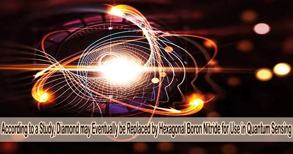
Due to its coherent nitrogen-vacancy centers, adjustable spin, sensitivity to magnetic fields, and ability to be employed at room temperature, diamond has long been the preferred material for quantum sensing. There hasn’t been much interest in researching diamond substitutes because such a suitable material is so simple to make and scale.
But there is one weakness in this GOAT of the quantum world. It is excessively large. Diamond is not the best material to study quantum sensors and information processing, just as an NFL linebacker is not the best athlete to ride in the Kentucky Derby. Diamonds’ vaunted super-stable flaw starts to disintegrate when they are too small. Diamond has a point at which it is no longer useful.
Enter hBN
hBN has previously been overlooked as a quantum sensor and a platform for quantum information processing. This recently altered as a result of the discovery of many novel flaws that are shaping up to be strong rivals to diamond’s nitrogen vacancy centers.
Of these the boron vacancy center (a single missing atom in the hBN crystal lattice) has emerged as the most promising to date. But only the -1 charge state, out of the many charge states, is appropriate for spin-based applications.
The other charge states have, so far, been challenging to detect and study. This was a concern since the charge state is unstable and can flicker between the -1 and 0 states, which is characteristic of environments for quantum sensors and devices.
This research shows that hBN has the potential to replace diamond as the preferential material for quantum sensing and quantum information processing because we can stabilize the atomic defects that underpin these applications resulting in 2D hBN layers that could be integrated into devices where diamond can’t be.
Angus Gale
But as outlined in a paper published in Nano Letters, researchers from TMOS, the ARC Center of Excellence for Transformative Meta-Optical Systems have developed a method to stabilize the –1 state, and a new experimental approach for studying the charge states of defects in hBNusing optical excitation and concurrent electron beam irradiation.
Co-lead author Angus Gale says, “This research shows that hBN has the potential to replace diamond as the preferential material for quantum sensing and quantum information processing because we can stabilize the atomic defects that underpin these applications resulting in 2D hBN layers that could be integrated into devices where diamond can’t be.”
Co-lead author Dominic Scognamiglio says, “We’ve characterized this material and discovered unique and very cool properties, but the study of hBN is in its early days. There are no other publications on charge state switching, manipulation or stability of boron vacancies, which is why we’re taking the first step in filling this literature gap and understanding this material better.”
Chief Investigator Milos Toth says, “The next phase of this research will focus on pump-probe measurements that will allow us to optimize defects in hBN for applications in sensing and integrated quantum photonics.”
Quantum sensing is a rapidly advancing field. Quantum sensors compared to traditional ones promise better sensitivity and spatial resolution. Precision temperature as well as electric and magnetic field sensing in microelectronic devices is one of its numerous applications that has drawn the most criticism for Industry 4.0 and the continued shrinking of gadgets. Controlling them requires being able to sense these.
One of the reasons currently preventing tiny electronics from performing even better is thermal management. Precision quantum sensing at the nanoscale will enhance performance and reliability while assisting in preventing microchip overheating.
Quantum sensing has important uses in the field of medical technology as well. For example, due to its capacity to detect magnetic nanoparticles and molecules, it may one day be used as an injectable diagnostic tool to look for cancer cells or to track the metabolic activity of cells to determine the effectiveness of medical treatments.
The TMOS team developed a new experimental setup that combined a confocal photoluminescent microscope with a scanning electron microscope (SEM) to analyze the boron vacancy defects in hBN. As a result, they were able to measure the defect and control the charge states of boron vacancy defects using both the electron beam and electrical microcircuits.
Gale says, “The approach is novel in that it allows us to focus the laser onto and image individual defects in hBN, while they are manipulated using electronic circuits and using an electron beam. This modification to the microscope is unique; it was incredibly useful and streamlined our workflow significantly.”
Manipulating the charge state of spin defects in hexagonal boron nitride
Negatively charged boron vacancies (VB−) in hexagonal boron nitride (hBN) have recently gained interest as spin defects for quantum information processing and quantum sensing by a layered material.
However, the boron vacancy can exist in a number of charge states in the hBN lattice, but only the -1 state has spin-dependent photoluminescence and acts as a spin-photon interface. Here, we investigate charge state switching of VB defects under laser and electron beam excitation.
We demonstrate deterministic, reversible switching between the -1 and 0 states (VB−⇌VB0 +e−), occurring at rates controlled by excess electrons or holes injected into hBN by a layered heterostructure device. Our technique offers a way to control the VB charge state and stabilize the -1 state, both of which are necessary for manipulating optical spins and reading out defects.