The ability to direct light from one location to another is the foundation of our modern civilization. Fiber optic cables transport light that encodes anything from YouTube movies to banking data beneath the oceans and across continents—all inside strands roughly the size of a hair.
Prof. Jiwoong Park of the University of Chicago, on the other hand, pondered what would happen if you built even thinner and flatter strands—so thin that they’re actually 2D instead of 3D. What would become of the light?
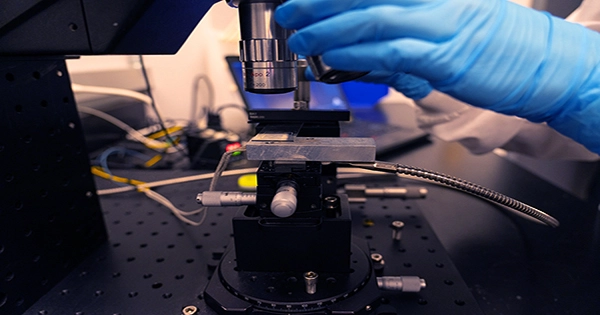
He and his colleagues discovered that a sheet of glass crystal only a few atoms thick could catch and convey light through a series of novel tests. Not only that, but it was surprisingly efficient and could go pretty great distances—up to a centimeter in the domain of light-based computing, which is rather far.
The study, published in Science, shows what are basically 2D photonic circuits and could pave the way for new technology.
“We were utterly surprised by how powerful this super-thin crystal is; not only can it hold energy, but it can deliver it a thousand times further than anyone has seen in similar systems,” said Jiwoong Park, lead study author and professor and chair of chemistry, as well as a member of the James Franck Institute and the Pritzker School of Molecular Engineering. “The trapped light also behaved as if it were moving in 2D space.”
Guiding light
The newly created technique is a two-dimensional method of guiding light known as a waveguide. During experiments, the researchers discovered that they could employ incredibly small prisms, lenses, and switches to guide the flow of light along a chip—everything needed for circuits and computations.
Existing photonic circuits are substantially larger and three-dimensional. Importantly, in existing waveguides, light particles known as photons always travel encapsulated within the waveguide.
The glass crystal in this system, the scientists noted, is actually thinner than the photon itself, so a portion of the photon actually sticks out of the crystal as it travels.
It’s similar to the difference between creating a tube to transport bags through an airport and placing them on top of a conveyer belt. The suitcases are open to the air on a conveyer belt, allowing you to readily see and adjust them en route. Because light can be easily moved with lenses or prisms, this approach makes it much easier to design sophisticated devices with glass crystals.
Photons can also gather information about the conditions as they travel. Consider examining the suitcases coming in from outside to see whether it is snowing. Similarly, scientists can envision employing these waveguides to create minuscule sensors.
“For example, suppose you had a sample of liquid and wanted to detect the presence of a specific molecule,” Park added. “You could design it so that this waveguide travels through the sample, and the presence of that molecule would change how the light behaves.”
The researchers are also interested in developing ultra-thin photonic circuits that can be layered to integrate many more small devices into the same chip area. Although the glass crystal employed in these studies was molybdenum disulfide, the principles should apply to other materials as well.
Though theoretical experts predicted that this behavior would exist, the scientists noted that actually observing it in the laboratory took years.
“It was a really difficult but rewarding problem because we were entering a completely new field.” “Everything we needed, from growing material to measuring how the light moved, we had to invent ourselves,” said graduate student Hanyu Hong, co-first author of the research.