Researchers can now analyze magnetic nanostructures with great resolution thanks to a novel technique. It was created by scientists from the Max Planck Institute of Microstructure Physics in Halle and Martin Luther University Halle-Wittenberg (MLU).
While standard light microscopes only have a resolution of 500 nanometers, the new technique obtains a precision of about 70 nanometers. This outcome is crucial for the creation of novel, energy-efficient spin electronics-based storage solutions. The current issue of the journal ACS Nano features the team’s research paper.
The wavelength of light limits the resolution of normal optical microscopes, making it unable to see details below 500 nanometers. By employing a metallic nano-scale tip and the anomalous Nernst effect (ANE), the novel technique gets beyond this restriction. In a magnetic metal, ANE produces an electrical voltage perpendicular to the temperature gradient and magnetization.
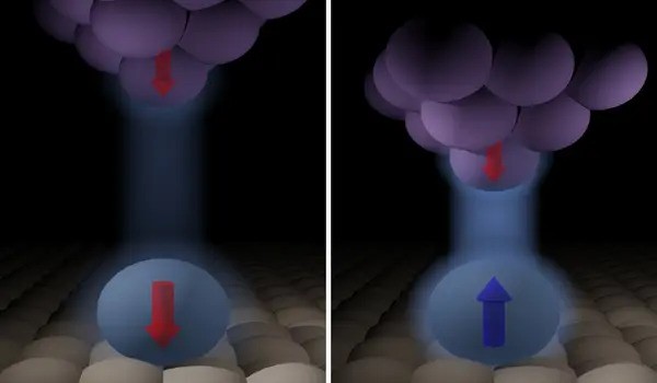
A laser beam focuses on the tip of a force microscope and thus causes a temperature gradient on the surface of the sample that is spatially limited to the nanoscale. The metallic tip acts like an antenna and focusses the electromagnetic field in a tiny area below its apex.
Professor Georg Woltersdorf
“A laser beam focuses on the tip of a force microscope and thus causes a temperature gradient on the surface of the sample that is spatially limited to the nanoscale,” says Professor Georg Woltersdorf from the Institute of Physics at MLU. “The metallic tip acts like an antenna and focusses the electromagnetic field in a tiny area below its apex.” This enables ANE measurements with a much better resolution than conventional light microscopy allows. The microscopic images published by the research team achieve a resolution of around 70 nanometres.
Magnetic polarization has only been examined in the sample plane in earlier research. The research team asserts that the in-plane temperature gradient is also essential since it enables the use of ANE measurements to examine the out-of-plane polarization. The researchers employed a magnetic vortex structure to bridge this gap and show the accuracy of the ANE approach for visualizing magnetic structures at the nanometer scale.

A particular advantage of the new technique is that it also works with chiral antiferromagnetic materials. “Our findings are significant for the thermoelectric imaging of spintronic components. We have already demonstrated this with chiral antiferromagnets,” says Woltersdorf.
“With our method has two advantages: on the one hand, we have greatly improved the spatial resolution of magnetic structures, far beyond the possibilities of optical methods. Secondly, it can also be applied to chiral antiferromagnetic systems, which will directly benefit our planned Cluster of Excellence ‘Centre for Chiral Electronics’,” says Woltersdorf.
Together with Freie Universität Berlin, the University of Regensburg and the Max Planck Institute of Microstructure Physics in Halle, MLU is applying for funding as part of the Excellence Strategy. The aim of the research is to lay the foundations for new concepts for the electronics of the future.


