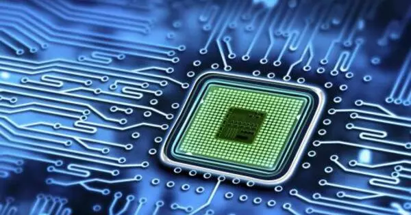
The process of creating miniature structures on micrometre scales or smaller is known as microfabrication. It is the process of creating structures, devices, or patterns on a micrometer or nanometer scale. Historically, the earliest microfabrication processes were used for integrated circuit fabrication, also known as “semiconductor manufacturing” or “semiconductor device fabrication”. It entails the fabrication and manipulation of materials and components in order to create intricate and precise structures for use in fields such as electronics, photonics, microfluidics, and biomedical engineering.
Microelectromechanical systems (MEMS), microsystems (European terminology), micromachines (Japanese terminology), and their subfields, microfluidics/lab-on-a-chip, optical MEMS (also called MOEMS), RF MEMS, PowerMEMS, BioMEMS, and their extension into nanoscale (for example, NEMS, for nano electro mechanical systems) have re-used, adapted, or extended microfabrication methods over the last two decades. Similar techniques are used in flat-panel displays and solar cells.
Microfabrication techniques allow for the creation of miniature devices with features and functionalities that would be impossible to achieve using traditional manufacturing processes. To create complex structures on a small scale, these techniques frequently employ a combination of processes such as lithography, deposition, etching, and bonding.
Here are some key processes commonly used in microfabrication:
- Lithography: It is a fundamental microfabrication process that involves patterning a photosensitive material known as a resist with light or electron beams. A pattern is created by selectively exposing the resist, which is then transferred to the underlying material via etching or deposition.
- Deposition: Thin films of materials are deposited onto a substrate in this process. Metal, semiconductor, and insulating material layers are commonly created using techniques such as physical vapor deposition (PVD), chemical vapor deposition (CVD), and atomic layer deposition (ALD).
- Etching: Etching is a technique for removing material from a substrate selectively in order to create desired patterns or structures. Wet etching involves immersing the substrate in a chemical solution, whereas dry etching methods use plasma to remove material, such as reactive-ion etching (RIE).
- Bonding: Microfabrication frequently necessitates the assembly of various components or layers. Thermal bonding, anodic bonding, and adhesive bonding are all techniques used to create permanent or temporary bonds between materials.
- Doping: Doping is the process of introducing impurities into a material to alter its electrical or optical properties. In microfabrication, dopants are often introduced into semiconductors to create regions with different conductivity types, enabling the fabrication of electronic devices such as transistors.
- Metrology: Metrology refers to the measurement and characterization of microfabricated structures and devices. Various techniques like scanning electron microscopy (SEM), atomic force microscopy (AFM), and optical microscopy are used to inspect and analyze the dimensions, surface features, and material properties.
Application
Microfabrication is critical in the development of miniaturized electronic devices, microelectromechanical systems (MEMS), lab-on-a-chip devices, sensors, integrated circuits, and a variety of other applications that require precise control and manipulation on a small scale.
Miniaturization of various devices poses challenges in a wide range of scientific and engineering fields, including physics, chemistry, materials science, computer science, ultra-precision engineering, fabrication processes, and equipment design. It is also spawning various types of interdisciplinary research. Microlithography, doping, thin films, etching, bonding, and polishing are the major concepts and principles of microfabrication.


