Ion implantation is a materials engineering process that involves the use of ionized atoms to modify the properties of a material. In this process, high-energy ions are accelerated and then directed towards a target material, where they are implanted into the surface layers of the material.
Ion implantation is a low-temperature process that accelerates ions of one element into a solid target, changing its physical, chemical, or electrical properties. Ion implantation is used in the fabrication of semiconductor devices, metal finishing, and materials science research. If the ions stop and remain in the target, they can change the elemental composition of the target (if their composition differs from the target’s).
When ions collide with a target at high energy, they cause chemical and physical changes. The energetic collision cascades can damage or even destroy the target’s crystal structure, and ions with sufficient energy (tens of MeV) can cause nuclear transmutation.
The energy of the ion beam determines the depth of the implanted ions, while the dose, or the number of ions implanted per unit area, determines the concentration of the implanted species. The implantation process can be used to create a variety of desired effects, including changing the electrical conductivity, introducing new chemical species, altering the mechanical properties, or modifying the surface topography of a material.
General principle
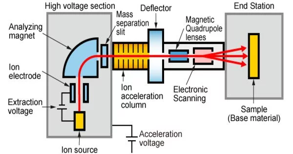
Ion implantation equipment typically consists of an ion source, which produces ions of the desired element, an accelerator, which electrostatically accelerates the ions to high energy or uses radiofrequency, and a target chamber, which allows the ions to impinge on a target, which is the material to be implanted. As a result, ion implantation is a subset of particle radiation.
Because each ion is typically a single atom or molecule, the actual amount of material implanted in the target is the integral of the ion current over time. This is referred to as the dose. Because implant currents are typically small (micro-amperes), the dose that can be implanted in a reasonable amount of time is small. Therefore, ion implantation finds application in cases where the amount of chemical change required is small.
Application
The process of ion implantation can be used to modify a wide range of materials, including semiconductors, metals, and polymers. It is commonly used in the semiconductor industry to introduce dopants into silicon wafers to create p-type or n-type regions, which are used to form the transistors and other components of integrated circuits.
Ion implantation is a precise and controllable process that can be used to create complex, three-dimensional structures with high precision and accuracy. However, it is also a relatively expensive process that requires specialized equipment and expertise.