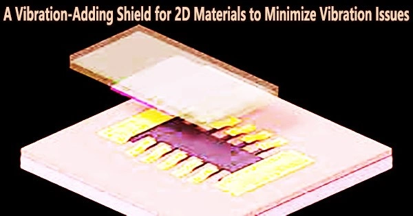
Researchers from Monash University have revealed a novel, paradoxical method to safeguard atomically thin electronics by reducing vibrations while boosting vibrations.
Gallium-oxide, a protective glass coating, is applied on graphene devices by “squeezing” a tiny droplet of liquid gallium.
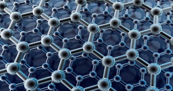
This oxide is potentially useful for industrial large-scale production since it is incredibly thin less than 100 atoms thick and covers scales that are centimeter wide. Current, frontier “2nm” transistors from IBM use gates of similar thickness, close to 10nm (140 atoms).
“Mechanically transferring such large-area nanosheets is quite novel,” says lead author Matthew Gebert.
The oxide provides a new method of device protection, whilst also improving device performance:
“The oxide not only enhances and protects our devices when we first transfer it, but also later, during subsequent processing and fabrication,” says co-author Semonti Bhattacharyya.
Gallium-improved oxide’s performance can be attributed in part to its high-K dielectric characteristics, which are crucial in the protracted process of miniaturizing devices and lowering power consumption.
A surprise outcome of protective gallium-oxide is the reduction of the electrical resistance in graphene that is brought on by thermal vibrations brought on by heat in the surrounding materials.
“That’s surprising because in effect we are actually adding extra vibrations, to reduce total vibrations,” says Matt.
This is the first instance where a graphene device has used such a method to lessen resistance brought on by thermal vibrations.
Protection from a Damaging Environment
The Monash team from the ARC Centre of Excellence in Future Low-Energy Electronics Technologies (FLEET) used a novel liquid-metal printing technique to create gallium-oxide (Ga2O3) glass. FLEET collaborators at RMIT, who have used the novel glass in a variety of electronics applications, designed this method.
The fence (the 2D graphene) is affected by the actions of neighbours on both sides (the insulating materials on either side of graphene). One neighbour might have a clean environment on their side of the fence (a good insulator, with few phonons) but the other neighbour might have an overgrown garden that damages the fence (a bad insulator with strong phonons).
Matt Gebert
Although being more than 5,000 times thinner than a human hair, the glass film that forms on the surface of droplets of liquid gallium metal can be successfully “printed” from the surface of the metal to form uniform continuous layers over centimeter-sized areas.
The liquid-metal method offers two advantages to protect devices. While the transferred layer serves as a good barrier for future processing, the layer-printing technique prevents growth damage.
Because of its High-K dielectric properties, gallium-oxide encapsulation not only provides protection but also has the potential to improve performance. Since the creation of these materials frequently entails the bombardment of extremely energetic atoms, high-K dielectrics have proven to be difficult to combine with graphene.
As gallium-oxide encapsulation is a mechanical transfer technique (“think forklift stacking,” says Matthew Gebert), it is fundamentally different to alternative deposition methods (such as atomic layer deposition, evaporation, sputtering and vapor deposition) which have undesirable attributes such as high temperature requirements.
Because gallium metal is liquid close to room temperature (30oC), this process has a lot of advantages for industrial adoption. In fact, before further processing utilizing these other techniques, gallium-oxide can be utilized as a buffer layer.
By using commercially available growing equipment to test their graphene devices, the Monash researchers showed that gallium-oxide shielded the material from surface abrasion. The portions of graphene that were not coated by gallium-oxide were unaffected by the addition of another oxide layer, whereas those areas kept their properties.
Dielectric Layers and their Importance in Computing
Transistors, the tiny “switches” at the core of electronics and computers, perform best when electrically insulating (dielectric) materials are used. You can use your phone or computer because these dielectric materials enable a transistor to turn on or off without leaking power.
Electrons build up across the dielectric material to produce a voltage and “switch” the transistor. Thinner dielectrics, on the other hand, leak current, which reduces switching speed and wastes current as heat. High-K dielectrics are crucial because they improve the switch’s performance, enabling a decrease in current leakage and, as a result, energy waste.
However, even high-K dielectrics devices are not impervious to size. As electronic materials get smaller and thinner as we relentlessly march towards cramming-in more transistors (to obey Moore’s Law), materials become strongly influenced by the surfaces of neighbouring materials, often resulting in an drop of performance. This explains why graphene is often damaged by high-K dielectrics.
One of these degrading phenomena that occur at surfaces is material vibrations.
Vibration and Gallium-Oxide’s Advantage
Phonons are the heat-induced vibrations of materials that result in electrical resistance in materials. Electrical resistance results from the oscillations that these vibrations (phonons) create in the atoms of a solid. Flowing electrons then bounce off these oscillations and alter their course.
One reason graphene is such a desirable material for electronics is that the thermal vibrations of the carbon atoms in graphene themselves produce astonishingly low resistance.
However, the thin nature of graphene (just one atom thick) means that thermal vibrations in surrounding (remote) materials can have a large effect on electrons in graphene, and these are the predominant cause of electrical resistance in graphene at room temperature.
More phonons are excited when temperatures rise, increasing the resistance by scattering electrons.
“You can think of this scenario as a fence,” explains Matt Gebert, who is a PhD candidate at Monash University/FLEET.
“The fence (the 2D graphene) is affected by the actions of neighbours on both sides (the insulating materials on either side of graphene). One neighbour might have a clean environment on their side of the fence (a good insulator, with few phonons) but the other neighbour might have an overgrown garden that damages the fence (a bad insulator with strong phonons) …”
“So in the end, your fence (graphene) doesn’t serve the purpose it was intended to, perhaps not even forming a complete fence (electronic circuit) anymore!”
The scientists mechanically moved substantial portions onto graphene devices to examine the gallium-protective oxide’s properties.
Subsequent measurements confirmed that graphene’s electronic properties at various temperatures and electron populations were maintained ie, high electron mobility (a very useful property of a transistor) is preserved.
“Surprisingly, adding the layer of Ga2O3 glass reduces the electrical resistance in graphene that is due to phonon scattering,” explains Matt.
(This is true in a target range of temperatures, which is slightly below room temperature.)
“This is counter-intuitive, because by adding this material, you are introducing additional phonons. So you might think: the more phonons, the higher we would expect resistance to be!”
However, these results do agree with existing theories of phonons in insulators. Ga2O3 can change its atomic arrangement to ‘screen’ the electric field from phonons in the silicon-dioxide glass on the other side of graphene thanks to the fact that it is a powerful phonon host.
The fact that the powerful Ga2O3 phonons are modes that need a lot of energy to populate only helps the situation. As a result, Ga2O3 phonons only becomes active at higher temperatures (with more thermal energy) and this results in lower overall resistance in graphene until a temperature of -53oC (220 K). Gallium-oxide is picking up (only the) good vibrations.
New Avenues To Device Performance.
This method of decreasing overall phonon content is proven for the first time and could be utilized to find hybrid materials that perform better for 2D electronics at ambient temperature.
Current silicon technologies, which are being pushed to the quantum-scale limits, could work well with a comparable dielectric material with higher-energy phonon modes than Ga2O3.
The liquid-metal printing technique is a versatile method for industrial partners. Ga2O3 touch-printing can be done on large wafer-scale areas, is highly automatable, and has demonstrated good reproducibility, proving its suitability for industry adoption.
In comparison to alternative oxide deposition techniques that demand vast quantities of material or extremely high temperatures, gallium metal, which melts at a temperature of roughly 30oC, and the transfer apparatus are also less expensive.