Defects exist in all semiconductors, whether by design or by chance. Impurities, native defects, and extended defects are fundamental properties of defects that affect a wide range of applications. These technologically significant flaws could be introduced during the growth and processing processes. Recent developments have highlighted the importance of fundamentally understanding defects. Controlling defect populations can improve the efficiency of light-emitting diodes and solar cells, particularly those made of novel materials. Dopant spins and optically active centers have the potential to be used as building blocks in quantum computers.
Researchers have devised a novel method for manipulating defects in semiconductors. The research could lead to new forms of precision sensing or the transfer of quantum information between physically separate qubits, as well as a better understanding of charge transport in semiconductors.
Dopants are found primarily on substitutional sites in semiconductors, where they either provide free electrons (donors) or bind them (acceptors) to complete the valence-bond structure. The most successful concepts for describing dopant diffusion assume that substitutional dopants form mobile pairs with intrinsic point defects such as vacancies and self-interstitials.
The key was isolating the source defect, leaving only the nitrogen-vacancy. Another important consideration was to have a “clean” diamond with as few flaws as possible. Then, because of the long-range attractive Coulombic interaction between a defect and a hole, the probability of the charge going towards the target increases dramatically, allowing us to make our observations.
Artur Lozovoi
A new method for manipulating defects in semiconductors has been discovered by City College of New York researchers. The research could lead to new types of precision sensing, such as the transfer of quantum information between physically separate qubits, as well as a better understanding of charge transport in semiconductors.
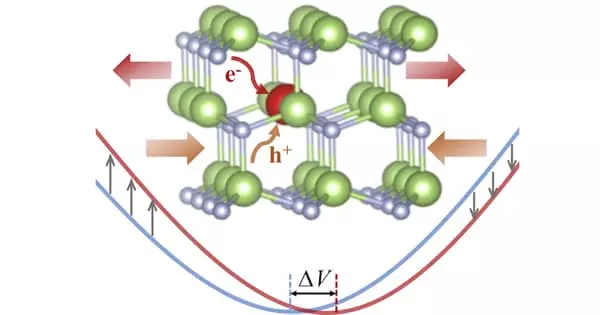
The researchers demonstrated that by using laser optics and confocal microscopy, they could make one defect eject charges, holes, under laser illumination, allowing the other defect several micrometers away to catch them. Charge capture is used to change the charge state of the latter defect from negative to neutral.
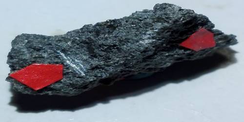
The nitrogen-vacancy center in diamond was used in the study as a special type of point defect. These color centers have spin, which is an inherent form of angular momentum carried by elementary particles, making them ideal for quantum sensing and processing. Based on the spin projection of the nitrogen-vacancy, the researchers used a specific protocol to filter out the charges that originated solely from it.
“The key was isolating the source defect, leaving only the nitrogen-vacancy,” said Artur Lozovoi, a physics postdoctoral researcher at CCNY’s Division of Science and the paper’s lead author. “Another important consideration was to have a “clean” diamond with as few flaws as possible. Then, because of the long-range attractive Coulombic interaction between a defect and a hole, the probability of the charge going towards the target increases dramatically, allowing us to make our observations.”
The researchers discovered that the charge transport efficiency in the clean material is a thousand times higher than in previous experiments, a phenomenon they refer to as a “giant capture cross-section.” This breakthrough could pave the way for a quantum information bus to be established between color center qubits in semiconductors.
“This charge capture process by a single defect has only been described theoretically before,” Lozovoi added. “We now have an experimental platform that allows us to investigate how these defects interact with free charges in crystals and how we can use it for quantum information processing,” says the researcher.
Understanding the formation and introduction mechanisms of defects in semiconductors is critical to understanding their properties, so this research focuses on that. Despite the fact that many defect-related issues have been identified and solved over the past 60 years of semiconductor research, the quest for faster, cheaper, lower-power, and new types of electronics necessitate the development of new materials and properties, posing new defect-related challenges.