Chemical Mechanical Polishing (CMP) is a process used in the semiconductor industry to flatten and smooth surfaces of a semiconductor wafer. It is also known as planarization, is a method of smoothing surfaces by combining chemical and mechanical forces. It is an essential step in the fabrication of integrated circuits and other electronic devices. It is a cross between chemical etching and free abrasive polishing.
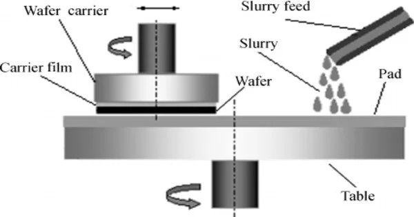
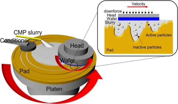
The process involves using a polishing pad, a slurry containing abrasive particles, and a chemical solution. The pad and slurry are used to mechanically remove material from the wafer’s surface, while the chemical solution reacts with the material to facilitate its removal. The process is typically performed on a rotating platen, which moves the wafer back and forth across the pad.
The abrasive particles in the slurry can be made from a variety of materials, including silica, alumina, diamond, and ceria. The chemical solution can also vary depending on the material being polished and the desired surface finish.
Description
An abrasive and corrosive chemical slurry (commonly a colloid) is used in conjunction with a polishing pad and retaining ring, which is typically larger in diameter than the wafer. A dynamic polishing head presses the pad and wafer together, which is held in place by a plastic retaining ring.
Different axes of rotation are used to rotate the dynamic polishing head (i.e., not concentric). This removes material and tends to even out any irregular topography, flattening or planarizing the wafer. This could be required to prepare the wafer for the formation of additional circuit elements. CMP, for example, can bring the entire surface into the depth of field of a photolithography system or remove material selectively based on its position. Typical depth-of-field requirements are down to Angstrom levels for the latest 22 nm technology.
Application
CMP can be used to achieve a variety of surface finishes, including flatness, roughness, and surface quality. It is particularly useful in producing a planarized surface, which is essential for creating high-quality integrated circuits. Overall, CMP plays a critical role in the semiconductor manufacturing process and is used extensively throughout the industry.
Shallow trench isolation (STI), a semiconductor device fabrication process, is a technique used to improve the isolation between devices and active areas. Furthermore, because of its higher degree of planarity, STI is essential in photolithographic applications, depth of focus budget by decreasing minimum line width. To planarize shallow trenches, a common method such as the combination of resist etching-back (REB) and chemical mechanical polishing should be used (CMP).
Limitations
There are currently several CMP limitations that emerge during the polishing process, necessitating the optimization of a new technology. Wafer metrology, in particular, requires improvement. Furthermore, several potential flaws in the CMP process were discovered, including stress cracking, delamination at weak interfaces, and corrosive attacks from slurry chemicals. The oxide polishing process, which is the oldest and most widely used in the industry today, has one drawback: the lack of end points necessitates blind polishing, making it difficult to determine when the desired amount of material has been removed or the desired degree of planarization has been achieved.