Making transistors and other electronic components more efficient and small while utilizing easily accessible methods and materials is a major goal in the field of electronics engineering. Ferroelectric field effect transistors (FE-FETs), which resemble normal FETs but also contain ferroelectric materials, are among the transistors that have been discovered to be particularly promising.
Ferroelectric materials that can switch and store electrical charge are used to make the gate insulators in FE-FETs. Therefore, these ferroelectric-based transistors could also function as memory devices in addition to controlling the current flow in electrical devices like traditional FETs.
This dual function might be very helpful for computationally intensive applications, including running artificial intelligence (AI) models, as it might enable devices to support their operation better without using too much power. Despite their potential, FE-FETs have not yet been widely adopted, in part due to the difficulty of reliably producing them on a large scale using current techniques.
Researchers at University of Pennsylvania, Penn State University, and other universities worldwide recently introduced a strategy to create FE-FETs using similar processes to those currently employed to produce FETs. Their paper, published in Nature Nanotechnology, could pave the way toward the widespread adoption of these dual-function transistors.
“The main motivation behind our study was to demonstrate that both 2D semiconductor materials such as MoS2 and nitride ferroelectrics like AlScN (i.e., aluminum scandium nitride) are very attractive for realizing compact, low-power and fast non-volatile memory devices that can be directly integrated on Si CMOS technology in a back end of line (BEOL) process,” Deep Jariwala, one of the researchers who carried out the study, told Phys.org.
“We have been looking at 2D materials and AlScN for this application for some time now. Our present paper is a tour de force demonstration of materials scaled up to large areas and devices scaled down to very small dimensions and operating voltages.”
To truly see their advantage and performance gains in big data computing we will need to shrink these devices further. We are now working toward this, and as shown in another recent paper of ours, ferroelectric AlScN can be reliably made and switched at 5 nm thickness. Our next step will be to integrate 2D materials and make FE-FETs from 5 nm thick AlScN films to truly realize devices and achieve operation voltages that can be compatible with leading edge Si CMOS processors. At a FE-FET device level, we also need to do more work on improving metal/ 2D semiconductor contact resistance values and also make p-type FE-FET devices.
Deep Jariwala
FE-FETs could function as non-volatile memory components due to their capacity to hold and switch electrical charge practically indefinitely, even when a voltage applied at its gate electron is withdrawn.
The primary goal of the study by Jariwala and his colleagues was to prove that FE-FETs can successfully be integrated with silicon semiconductor materials and could thus be fabricated to support the high bandwidth memory demands of big data applications.
“The charge stored by FE-FETs also modulates the conductivity of the 2D semiconductor into a high or low resistance state which actually represents the information stored in the memory device,” Jariwala explained. “The key advantage of our strategy lies in the combination of AlScN ferroelectric material which has superlative ferroelectric properties and can be deposited in BEOL compatible processes and 2D semiconductors, which by virtue of their thin nature and van der Waals structure can allow strong modulation of the conductivity and can also be integrated with relative ease.”
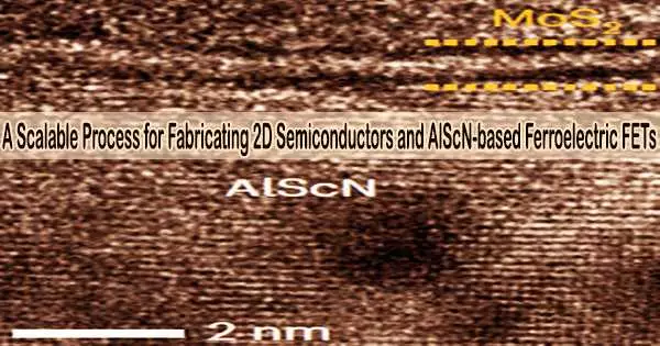
The researchers’ FE-FETs combine channels built of a 2D semiconductor and a ferroelectric substance known as AlScN, both of which were manufactured utilizing traditional, wafer-scalable techniques.
The team tested a large array of their FE-FETs in a series of tests and found that they performed remarkably well, exhibiting memory windows larger than 7.8 V, ON/OFF ratios greater than 107 and ON-current density greater than 250 μA um–1 at ~80 nm channel length.
“Our demonstration proves that 2D semiconductor/AlScN FE-FET devices are ready for integration with Si CMOS to bring big-data computing requiring high bandwidth memory with processors in future generations of computer hardware,” Jariwala said.
“Both these classes of materials are becoming mature, and our work creates a bridge for making this leap from the lab to the foundry, of these materials and memory devices.”
The recent work by Jariwala and his colleagues could soon contribute to the large-scale implementation of FE-FETs. The prototypes they have so far created switch voltage between 3 and 4 volts, have good data storage capabilities, and are simple to interface with some modern silicon CMOS processors. The scientists want to make them further smaller in their upcoming research since doing so would make it easier for them to be integrated into consumer electronics.
“To truly see their advantage and performance gains in big data computing we will need to shrink these devices further,” Jariwala added. “We are now working toward this, and as shown in another recent paper of ours, ferroelectric AlScN can be reliably made and switched at 5 nm thickness. Our next step will be to integrate 2D materials and make FE-FETs from 5 nm thick AlScN films to truly realize devices and achieve operation voltages that can be compatible with leading edge Si CMOS processors. At a FE-FET device level, we also need to do more work on improving metal/ 2D semiconductor contact resistance values and also make p-type FE-FET devices.”