Is it conceivable to create tiny and soft wearable devices with electrical and optical capabilities, similar to Spiderman’s suit?
The solution is to create innovative materials that outperform existing materials and to develop technology that allows for exact control of such materials’ physical properties.
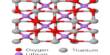
Separating transition metal dichalcogenide (TMD) into a single layer, similar to graphene, transforms it into a thin, two-dimensional (2D) film material with the properties of high-performance semiconductors. Different combinations of TMD types and stacking methods can produce unique properties by stacking two disparate TMD layers.
As a result, 2D semiconductors based on heterostructures are gaining traction as an important next-generation material for the electronics sector in academics and industries worldwide.
However, commercialization remains difficult due to the difficulty of precisely controlling the physical properties of their quasiparticles.
Professor Kyoung-Duck Park, Yeonjeong Koo, and Hyeongwoo Lee from the Department of Physics at POSTECH conducted joint research with the team from ITMO University in Russia led by Professor Vasily Kravtsov to develop a multifunctional tip-enhanced spectroscopy that dynamically controls the quasiparticles of a 2D material in a small space.
Using spectroscopy at the 20-nm level, the researchers successfully controlled semiconductor particles such as interlayer excitons and interlayer trions generated at TMD heterobilayers. The research was recently published in Light: Science & Applications.
The spectroscopy the team developed can be employed in identifying new physical properties of individual semiconductor particles such as interlayer excitons from the TMD heterobilayers. I am very much looking forward to the next physical discoveries.
Yeonjeong Koo
Like excitons, interlayer excitons of TMD heterobilayers exhibit photoluminescence (PL), which is one of the properties of semiconductor materials. Because they are part light and part matter, interlayer excitons, which are electrically neutral quasiparticles, can be used in next-generation semiconductor devices with less heat.
Because they have a longer coherence time than excitons, they can also be used as a light source in quantum information technologies. Nonetheless, there are several obstacles to overcome in their application. At room temperature, they have a relatively low luminous efficiency and it is difficult to control their luminous energy.
The POSTECH team led by Professor Park, which had proposed technology for controlling excitons in nano-scale spaces in its previous research, successfully developed the multifunctional tip-enhanced spectroscopy that can be adjusted by gigapascal (GPa)-scale pressure and near-field intensity.
The spectroscopy can boost the luminous efficiency of interlayer excitons by around 9,000 times and dynamically vary their luminous energy (the color of the light). Furthermore, the team used the tip-based hot electron-injection technology to achieve the world’s first dynamic control of quasiparticle conversion between interlayer excitons and interlayer trions.
The most significant benefit of the research breakthrough is that it enables dynamically controlling the physical properties of quasiparticles at room temperature and atmospheric pressure, as well as analyzing the optical properties of semiconductor particles in real time with a spatial resolution of about 20nm, which is far shorter than the wavelength of light.
Yeonjeong Koo, one of the two co-first authors of the research paper, explained, “The spectroscopy the team developed can be employed in identifying new physical properties of individual semiconductor particles such as interlayer excitons from the TMD heterobilayers. I am very much looking forward to the next physical discoveries.”
The findings of the study are expected to open up new avenues for numerous uses of 2D semiconductors based on heterostructures, which are being extensively researched as a next-generation material. The fact that basic research in measuring instrument development played a significant role in the conclusion drew even more attention in the field.
The technology will also be used to create high brightness, ultrathin wearable optoelectronic devices. The achievement is all the more meaningful in the current situation where the U.S., Japan, and China are vying for dominance in the semiconductor equipment market and putting up technology barriers.