While the hot topic among emerging technologies based on how matter and energy behave at the atomic and subatomic level appears to be quantum computing, another path promises to bring up new opportunities for scientific study itself: quantum microscopy.
New microscopy modalities that can observe electric currents, detect changing magnetic fields, and even view single molecules on a surface are now possible because to the development of quantum technology.
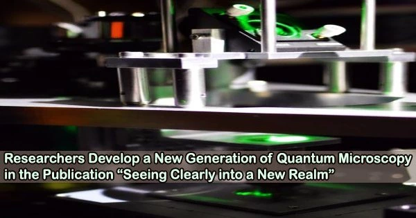
A prototype of such a microscope, demonstrating high resolution sensitivity, has been developed by an Australian research team headed by Professor Igor Aharonovich of the University of Technology Sydney and Dr. Jean-Philippe Tetienne of RMIT University. The team’s findings have now been published in Nature Physics.
The quantum microscope relies on atomic imperfections that, after being illuminated by a laser, emit light that can be directly linked to important physical characteristics like the magnetic field, electric field, or the chemical environment around the defect.
Professor Aharonovich praised the study team’s use of atomically thin layers known as hexagonal boron nitride (hBN) instead of the bulky crystals frequently used for quantum sensing as the innovative aspect of the new methodology.
There is a huge potential for this new generation of quantum microscopy. Not only can it operate at room temperature and provide simultaneous information on temperature, electric and magnetic fields, it can be seamlessly integrated into nanoscale devices and withstand very harsh environments, as hBN is a very rigid material.
Dr. Mehran Kianinia
“This van der Waals material that is, made up of strongly bonded two-dimensional layers can be made to be very thin and can conform to arbitrarily rough surfaces, thus enabling high resolution sensitivity,” Professor Aharonovich said.
“These properties led us to the idea of using ‘quantum-active’ hBN foils to perform quantum microscopy, which essentially is an imaging technique that utilises arrays of quantum sensors to create spatial maps of the quantities they are sensitive to,” Dr. Tetienne said.
“Until now, quantum microscopy has been limited in its spatial resolution and flexibility of application by the interfacing issues inherent in using a bulky three-dimensional sensor. By instead utilising a van der Waals sensor, we hope to extend the utility of quantum microscopy into arenas that were previously inaccessible.”
The scientists used a flake of CrTe2, a van der Waals ferromagnet with a critical temperature just above room temperature, as a technologically relevant magnetic material to test the prototype’s capabilities.
It was previously thought unachievable, yet the hBN-based quantum microscope was able to image the magnetic domains of the ferromagnet under ambient settings and with nanoscale proximity to the sensor.
Furthermore, a simultaneous temperature map was captured using the special qualities of the hBN flaws, demonstrating that the microscope may be utilized to carry out correlative imaging between the two values.
Lead authors for the Nature Physics paper, PhD students Alex Healey (University of Melbourne) and Sam Scholten (University of Melbourne), and early career researcher Tieshan Yang (UTS), said the van der Waals nature of the sensor had allowed the dual sensing of magnetic properties and temperature.
“Because it is very thin, not much heat is able to dissipate through it and any temperature distribution that exists is the same as if the sensor were not there,” they said. “What began as an experimental annoyance ended up being a hint towards a capability of our microscope that is unique among current alternatives.”
“There is a huge potential for this new generation of quantum microscopy,” UTS senior researcher Dr. Mehran Kianinia said. “Not only can it operate at room temperature and provide simultaneous information on temperature, electric and magnetic fields, it can be seamlessly integrated into nanoscale devices and withstand very harsh environments, as hBN is a very rigid material.”
“The main future applications include high resolution MRI (magnetic resonance imaging) and NMR (nuclear magnetic resonance) that can be used to study chemical reactions and identify molecular origins, as well as applications in space, defence and agriculture where remote sensing and imaging are key.”