A new all-optical method for driving multiple highly dense nanolaser arrays has been developed by researchers. The method could lead to chip-based optical communication links that process and move data faster than current electronic-based devices.
“The development of optical interconnects equipped with high-density nanolasers would improve information processing in data centers that move data across the internet,” said Korea University research team leader Myung-Ki Kim. “This could enable the streaming of ultra-high-definition movies, larger-scale interactive online encounters and games, the acceleration of the Internet of Things’ expansion, and the fast connectivity required for big data analytics.”
The researchers demonstrate in Optica, Optica Publishing Group’s journal for high-impact research, that densely integrated nanolaser arrays with lasers only 18 microns apart can be fully driven and programmed with light from a single optical fiber.
“Optical devices integrated onto a chip are a promising alternative to electronic integrated devices, which are struggling to meet today’s data processing demands,” Kim explained. “We reduced the overall dimensions of the laser array while also eliminating the heat generation and processing delays associated with electrode-based drivers by eliminating the large and complex electrodes typically used to drive laser arrays.”
Optical devices integrated onto a chip are a promising alternative to electronic integrated devices, which are struggling to meet today’s data processing demands. We reduced the overall dimensions of the laser array while also eliminating the heat generation and processing delays associated with electrode-based drivers by eliminating the large and complex electrodes typically used to drive laser arrays.
Myung-Ki Kim
Replacing electrodes with light
The new nanolasers could be used in optical integrated circuit systems, which detect, generate, transmit and process the information on a microchip via light. Instead of the fine copper wires used in electronic chips, optical circuits use optical waveguides, which allow much higher bandwidths while generating less heat. However, because the size of optical integrated circuits is quickly reaching into the nanometer regime, there is a need for new ways to drive and control their nano-sized light sources efficiently.
To emit light, lasers need to be supplied with energy in a process called pumping. For nanolaser arrays, this is typically accomplished using a pair of electrodes for each laser within an array, which requires significant on-chip space and energy consumption while also causing processing delays. To overcome this critical limitation, the researchers replaced these electrodes with a unique optical driver that creates programmable patterns of light via interference. This pump light travels through an optical fiber onto which nanolasers are printed.
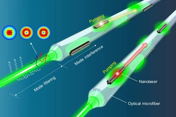
To demonstrate this approach, the researchers used a high-resolution transfer-printing technique to fabricate multiple photonic crystal nanolasers spaced 18 microns apart. These arrays were applied onto the surface of a 2-micron-diameter optical microfiber. This had to be done in a way that precisely aligned the nanolaser arrays with the interference pattern. The interference pattern could also be modified by adjusting the driving beam’s polarization and pulse width.
Laser driving with a single fiber
The experiments showed that the design allowed multiple nanolaser arrays to be driven using light traveling through a single fiber. The results matched well with numerical calculations and showed that the printed nanolaser arrays could be fully controlled by the pump beam interference patterns.
“Our all-optical laser driving and programming technology can also be applied to chip-based silicon photonics systems, which could play a key role in the development of chip-to-chip or on-chip optical interconnects,” said Kim. “However, it would be necessary to prove how independently the modes of a silicon waveguide can be controlled. If this can be done, it would be a huge leap forward in the advancement of on-chip optical interconnects and optical integrated circuits.”