A plasmonic-enhanced solar cell, also known as a plasmonic solar cell, is a type of solar cell (including thin-film or wafer-based cells) that converts light into electricity with the help of plasmons but where the photovoltaic effect occurs in a different material. It is a type of solar cell that uses plasmonic nanostructures to increase the efficiency with which sunlight is converted into electricity.
A direct plasmonic solar cell is a photovoltaic solar cell that uses plasmons as the active, photovoltaic material. Plasmonics is a subfield of nanophotonics that studies the interaction of an electromagnetic field with free electrons in a metal, referred to as surface plasmons. Plasmonic nanostructures can concentrate and enhance the electromagnetic fields near their surfaces, which can be exploited to enhance light absorption in solar cells.
The basic idea behind plasmonic-enhanced solar cells is to use these enhanced electromagnetic fields to improve light absorption, increase the generation of electron-hole pairs (excitons), and thus improve overall photovoltaic efficiency. The general procedure is as follows:
- Plasmonic Nanostructures: Plasmonic nanostructures are typically composed of metal nanoparticles (such as gold or silver) or metal thin films with localized surface plasmon resonances. These structures can be designed to interact with specific wavelengths of light, thereby enhancing the electromagnetic field around them.
- Light Absorption Enhancement: Plasmonic nanostructures are placed strategically within or on the surface of the solar cell. When sunlight strikes these nanostructures, the electromagnetic fields around them are concentrated. This increases light absorption in the nearby semiconductor material (typically silicon), increasing the number of photons absorbed and generating more electron-hole pairs.
- Hot Carrier Generation: Plasmonic nanostructures have the ability to generate “hot carriers.” When a photon is absorbed, it can produce an energetic electron-hole pair, with one of the carriers possessing significantly more energy than the semiconductor’s bandgap. These hot carriers may be captured before they lose their excess energy as heat, resulting in increased efficiency.
The active material thickness varies from that of traditional silicon PV (~100-200 μm wafers), to less than 2 μm thick, and theoretically could be as thin as 100 nm. The devices can be supported on substrates cheaper than silicon, such as glass, steel, plastic or other polymeric materials (e.g. paper).
Thin film solar cells face one challenge in that they do not absorb as much light as thicker solar cells made from materials with the same absorption coefficient. Light trapping techniques are critical for thin-film solar cells. Plasmonic-enhanced cells increase absorption by scattering light with metal nanoparticles excited at their surface plasmon resonance.
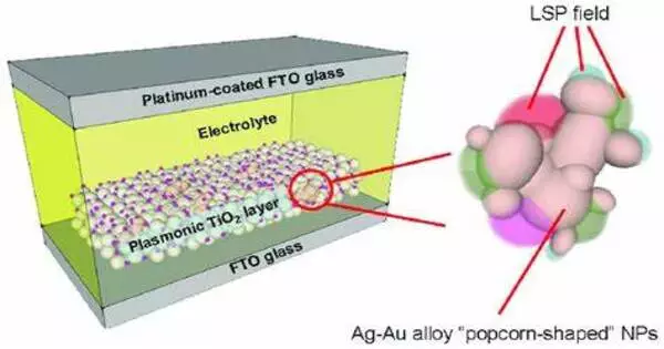
Direct plasmonic solar cells, on the other hand, take advantage of the fact that incoming light at the plasmon resonance frequency induces electron oscillations at the surface of the nanoparticles. A conductive layer can then capture the oscillation electrons, resulting in an electrical current. The voltage produced is determined by the conductive layer’s bandgap and the potential of the electrolyte in contact with the nanoparticles.