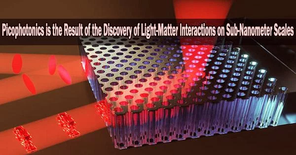
New waves with picometer-scale spatial fluctuations in electromagnetic fields have been found by Purdue University researchers, and they can go through semiconductors like silicon. The research team, led by Dr. Zubin Jacob, Elmore Associate Professor of Electrical and Computer Engineering and Department of Physics and Astronomy (courtesy), published their findings in APS Physics Review Applied in a paper titled, “Picophotonics: Anomalous Atomistic Waves in Silicon.”
“The word microscopic has its origins in the length scale of a micron which is a million times smaller than a meter. Our work is for light matter interaction within the picoscopic regime which is far smaller, where the discrete arrangement of atomic lattices changes light’s properties in surprising ways,” says Jacob.
These fascinating results show that a wide range of complex light-matter interaction events exist in natural media at the atomistic level. Researchers may devise fresh, useful optical devices as a result of the usage of picophotonic waves in semiconducting materials, enabling applications in quantum technologies.
Many photonic devices, including lasers and detectors, depend on the interaction of light and matter in materials. The past ten years have seen significant advancements in the field of nanophotonics, which examines how light moves within constructed structures like photonic crystals and metamaterials on a nanoscale scale.
We recently initiated the picoelectrodynamics theory network where we are bringing together diverse researchers to explore macroscopic phenomena stemming from microscopic pico-electrodynamic fields inside matter.
Dr. Zubin Jacob
This current research falls under the purview of the traditional hypothesis of atomic matter. A significant advance using a quantum theory of atomistic response in matter allowed for the recent discovery leading to picophotonics. The team consists of Jacob as well as Dr. Sathwik Bharadwaj, research scientist at Purdue University, and Dr. Todd Van Mechelen, former post-doc at Purdue University.
The gap between atomic lattices, their symmetries, and how they relate to intensely picoscopic light fields has long been a source of puzzlement in the area. The theory team created a Maxwell Hamiltonian framework of matter along with a quantum theory of light-induced response in materials to solve this conundrum.
“This is a pivotal shift from the classical treatment of light flow applied in nanophotonics,” says Jacob. “The quantum nature of light’s behavior in materials is the key for the emergence of picophotonics phenomena.”
Bharadwaj and colleagues demonstrated that in the atomic lattice, new anomalous waves appear among the conventional, well-known electromagnetic waves. Even within one of the silicon crystal’s (sub-nanometer length scale) core building blocks, these light waves exhibit strong oscillation.
“Natural materials itself have rich intrinsic crystal lattice symmetries and light is strongly influenced by these symmetries,” says Bharadwaj. “The immediate next goal is to apply our theory to the plethora of quantum and topological materials and also verify the existence of these new waves experimentally.”
“Our group has been leading the frontier of research on pico-scale electrodynamic fields inside matter at the atomistic level,” says Jacob. “We recently initiated the picoelectrodynamics theory network where we are bringing together diverse researchers to explore macroscopic phenomena stemming from microscopic pico-electrodynamic fields inside matter.”
This research was funded by the DARPA QUEST program.


