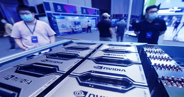
ANALYSIS Nvidia has emerged as the clear winner in the race to capitalize on the potential of generative AI, more than doubling its year-over-year revenues in Q2 alone. To maintain its dominance, the GPU behemoth appears to want to accelerate the development of new accelerators.
For several generations, a two-year cadence was sufficient to maintain a competitive edge. However, according to slides [PDF] from an investor presentation earlier this month, the B100 will be joined by a new “Super Chip” combining Arm cores with the Blackwell architecture, as well as a replacement for the L40 and L40S.
There are no major shocks here; we all expected to hear about Nvidia’s next-generation architecture and the B100 in its different versions around 2024.
According to the presentations, Nvidia will switch to a one-year release cycle. According to the presentation, the Blackwell-based B100 and its contemporaries will be replaced in 2025 by a “X100” class of parts. While Huang considers which mathematician, computer scientist, or engineer to dedicate the architecture to, we’ll assume “X” is a placeholder. However, the point remains: Nvidia aims to release new GPUs quickly.
What does this mean for Intel and AMD?
The move may pose a dilemma for companies such as AMD and Intel, which continue to release GPUs and AI accelerators every two years.
AMD, for example, released its Instinct MI200-series accelerators around a year after Nvidia’s A100, boasting significantly greater double-precision performance and equivalent FP16 FLOPS if you ignored Nvidia’s sparsity support.
When compared to the A100, the former gives the corporation a distinct advantage in high-performance computing applications, thus it’s no surprise that it’s become such a popular component in supercomputers like Europe’s Lumi or the Department of Energy’s Frontier Supercomputers.
AMD intends to challenge Nvidia’s dominance in the AI area with GPUs and APUs better tailored for lower precision workloads now that generative AI is whipping up demand. However, if the performance estimates for the MI300A/X compiled by our sister site The Next Platform are correct, AMD’s latest chips may not be FLOPS competitive with the H100, but they may have a memory edge. The processors are expected to feature 128GB-192GB of HBM3 memory, giving them a slight advantage over the H100.
Intel, which touted AI at its Innovation conference in September, is in a similar situation. The company had already adopted an accelerated release cadence for CPUs and GPUs but backed out of the latter due to division restructuring and cost-cutting efforts.
This decision led to the termination of both the XPU CPU-GPU architecture and Rialto Bridge, the replacement of the Ponte Vecchio accelerators that power the Aurora supercomputer at Argonne National Lab. The business then postponed the launch of its redesigned Falcon Shores from 2024 to 2025, claiming that the move “matches customer expectations on new product introductions and allows time to develop their ecosystems.”
The latter is intriguing because it will combine Intel’s GPU Max and Habana Labs technologies into a single platform. Until then, we’ll have to make do with Intel’s Gaudi2 and GPU Max families until Gaudi3 arrives.
Gaudi2 outperformed the A100 in terms of performance, but by the time it was released last year, Nvidia’s more capable H100 had already been announced and was months away from release.
Habana’s next-generation accelerator, Gaudi3, appears promising, but it will have to outperform not just the H100 and AMD’s MI300-series parts, but also the upcoming debut of Nvidia’s B100 accelerators.
This doesn’t mean that MI300 or Gaudi3 will be dead on arrival; rather, their window of usefulness may be significantly shorter than in the past, according to SemiAnalysis creator Dylan Patel, who was among the first to notice the hastened roadmap.
“There is a window where MI300 is the best chip on the market,” he said, adding that while we don’t know nearly as much about Intel’s Gaudi3 if it scales as well as he thinks, it will outperform Nvidia’s H100.
In the long run, he expects Intel and AMD to follow suit and accelerate their own GPU and accelerator research roadmaps.
And, as we’ve already stated, even if Intel and AMD’s next-generation accelerators can’t beat Nvidia, they may end up winning merely on availability. The availability of advanced packaging technology provided by TSMC is apparently limiting Nvidia’s H100s. This shortfall is not likely to be resolved until 2024. While AMD’s MI300-series chips, which also use these advanced packing techniques, are expected to face similar issues, Intel has the capability to build its own packaging, though it’s unclear whether Gaudi3 actually uses it, or if they’re in the same boat as Nvidia and AMD.
Not just about the accelerators: However, it is worth emphasizing that Nvidia is not simply speeding up the release frequency of its accelerators. It is also expanding its Quantum Infiniband and Spectrum Ethernet switching products.
While a single GPU is capable, AI training and HPC applications typically require huge clusters of accelerators to run properly, which requires networking that can keep up with them.
Nvidia gained ownership of its network stack, which comprises the company’s switching and NIC portfolios after it acquired long-time partner Mellanox in 2020.
Nvidia’s fastest switches now peak out at 25.6Tbps for Infiniband and 51.2Tbps for Ethernet. That bandwidth is distributed among a number of 200-400Gbps ports. Nvidia, on the other hand, plans to increase port speeds to 800Gbps in 2024 and 1,600Gbps in 2025 under this new release cycle.
This will demand not only more competent switch silicon with capacities ranging from 51.2 to 102.4Tbps but also quicker 200Gbps serializer/deserializers (SerDes) to accommodate 1,600Gbps QSFP-DD modules.
This degree of network performance is already possible thanks to existing technology. Broadcom has already shown 200Gbps SerDes. However, we have yet to see it from Nvidia. And, as Patel points out, Nvidia will ideally aim to reach 102.4Tbps on both Infiniband and Ethernet to fully benefit on 800Gbps capable NICs.
A PCIe problem: This is where Nvidia’s master strategy may begin to unravel. Due to PCIe restrictions, these higher speeds may not be possible on such a short timetable with existing NICs. A single 400Gbps port is currently the realistic limit for a NIC. PCIe 6.0 should get us to 800 Gbps, but we’ll need PCIe 7.0 to seriously consider 1,600 Gbps.
We already know that Intel’s next-generation Xeons will not support PCIe 6.0 when they ship in 2024, and we don’t know enough about AMD’s future Turin Epycs to predict whether they will. Despite the fact that AMD has led Intel in the adoption of new PCIe standards over the last few generations.
Nvidia, meanwhile, does not limit itself to x86. Now, the company has its own Arm-based CPUs. So perhaps Nvidia intends to support PCIe 6.0 on the Grace replacement. Arm chips were among the first to add PCIe 5.0 capability in early 2022, so there’s reason to expect the same thing will happen again.
Because of this issue, Patel anticipates that the B100 will have two variants. One that is PCIe 5.0 compatible and has the same 700-watt thermal design power (TDP) as the H100, allowing users to install a new HGX motherboard into their existing chassis designs. The second, he believes, will be significantly more powerful, require liquid cooling, and use PCIe 6.0.
However, when you start talking about 1,600 Gbps ports, as Nvidia intends to do in 2025, you’ll require PCIe 7.0, which has yet to be finalized. “You talk to the standards body, nobody expects anything PCIe 7.0 until 2026 at the earliest for products,” he went on to say. “It’s just impossible to do on that timeline.”
The alternative solution is to avoid using the PCIe bus. According to Patel, Nvidia does not require PCIe 6.0 or PCIe 7.0 levels of bandwidth between the GPU and CPU, only between the NIC and GPU. As a result, he anticipates that Nvidia will mostly avoid using the CPU as a bottleneck.
In fact, Nvidia is already doing some of this. Nvidia has basically daisy-linked the GPUs off their ConnectX NICs in more recent generations by employing a PCIe switch. According to Patel, Nvidia is likely to expand on this strategy in order to attain port speeds greater than what a single PCIe 5.0 or PCIe 6.0 x16 slot could normally support.
In terms of the X100 generation, he claims that there are reports that Nvidia would abandon PCIe for communications between the NIC and GPU in 2025 in favor of their own interconnect.
Those who have been following Nvidia’s AI efforts may be asking where the chipmaker’s super-high-bandwidth NVLinks fabric fits in. The technology is used to connect numerous GPUs so that they function as if they were one large one. With the addition of an NVLink switch, you can extend to numerous nodes.
However, NVLink has several important limits, particularly in terms of reach and scalability. While NVLink is far quicker than both, it is also limited to 256 devices. To go beyond this, you’ll need to use Infiniband or Ethernet to connect new clusters.
NVLink mesh is similarly limited to GPU-to-GPU communication. It will not help with data entry and output or workload coordination.
As a result, whether or not Nvidia is successful in shortening its release timeline will be strongly dependent on getting networking to scale quickly enough to avoid choking its chips.