Ion implantation is a low-temperature procedure that accelerates ions of one element into a solid target, modifying its physical, chemical, or electrical properties. It is a materials engineering method that involves the introduction of dopant atoms or other foreign atoms into the crystal lattice of a semiconductor wafer or other solid material. Ion implantation is utilized in the manufacture of semiconductor devices, metal finishing, and materials science research. This procedure is required for the manufacture of integrated circuits and other semiconductor devices.
Here’s a breakdown of how ion implantation works:
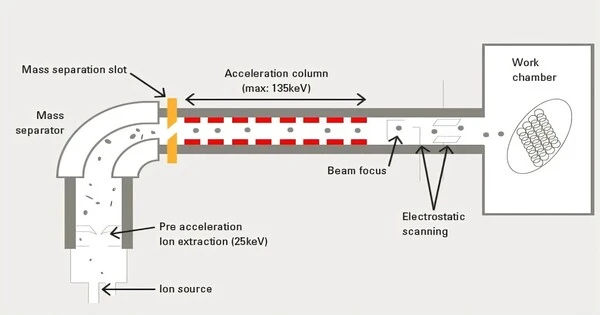
- Ion Selection: The initial step is to choose the right type of ions (charged atoms) for implantation. Typically, these ions are chosen to impart specific electrical or structural features into the target material. Depending on the required properties, common ions include boron, phosphorus, arsenic, and others.
- Ion Generation: Ion beams are created with sophisticated equipment known as ion implanters. Gas sources containing the desired dopant elements are ionized in these devices, resulting in a stream of ions. An electric field is then used to accelerate the ions to high energies.
- Ion Implantation: The high-energy ion beam is directed at the surface of the target material, typically a silicon wafer for semiconductor fabrication. As the ions penetrate the material, they lose energy and eventually come to a stop within the crystal lattice.
- Implantation Depth Control: The depth to which the ions penetrate the material can be controlled by adjusting the energy of the ion beam. This allows for precise doping profiles within the material.
- Annealing: After ion implantation, the wafer is often subjected to an annealing process, which involves heating the material to high temperatures. Annealing helps to repair any damage caused by the ion bombardment and activates the dopant atoms, incorporating them into the crystal lattice.
If the ions halt and remain in the target, they can change the elemental composition of the target (if their composition differs from that of the target). When high-energy ions strike a target, they trigger chemical and physical changes. The powerful collision cascades can damage or even destroy the target’s crystal structure, and ions with enough energy (tens of MeV) can cause nuclear transmutation.
Ion implantation offers several advantages for semiconductor device manufacturing:
- Precise Doping: It allows for very precise control over the concentration and depth of dopant atoms, enabling the creation of complex doping profiles in semiconductor materials.
- Uniformity: Ion implantation can achieve a high degree of uniformity across large semiconductor wafers, ensuring consistent device performance.
- Low Temperature: Unlike some other doping techniques, ion implantation is a relatively low-temperature process, which minimizes thermal stress on the semiconductor material.
- Selective Doping: Different regions of a wafer can be selectively doped with different types of ions, enabling the creation of various electronic components on a single chip.
- Reduced Contamination: It minimizes contamination from the dopant source, which can be a concern in other doping methods.
Ion implantation is a crucial step in the production of modern semiconductor devices, allowing for the precise control of electrical properties and the creation of complex integrated circuits.