The way we communicate now is governed by lasers, which produce light in a single direction with photons moving at a single frequency and all with the same phase (coherent).
Although most people think of lasers as little torches that shoot high-purity color beams, the workhorse of lasers is in the infrared spectrum, which human eyes cannot see. This is due to optical fibers’ high infrared transparency (1.3-1.6 um), which allows for effective optical transmission at very high data speeds.
Furthermore, infrared lasers have minimal ambient light overlap and are deemed eye-safe, allowing them to be used in LIDAR (light detection and ranging) applications such as 3D imaging, automotive, and free-space communications.
Infrared lasers are now mostly constructed of Erbium-doped fibers or III-V epitaxial semiconductors, which limits their manufacture and simple integration with electronics.
Due to the indirect bandgap of silicon, light sources (lasers, the engine of photonic components) are difficult to build in silicon photonics (SiPh) (a horizontal shift between the valence and conduction band of the material). A material must have a straight bandgap in order to create light.
The results of this study are considered a major breakthrough in the field of CQD optoelectronics. This discovery may facilitate fully integrated silicon photonics, paving the way towards low-cost solution-processed and CMOS integrated lasing sources for on-chip comm or LIDAR applications. Prior to demonstrating lasing under continuous-wave or nanosecond stimulation, which is our next milestone, further work must be done to improve the material.
Prof. Gerasimos Konstantatos
As a result, additional direct bandgap materials, such as indium phosphide (InP), are utilized to make the lasers, which are then incorporated into the SiPh wafer (chip) to power the photonic components inside the photonic circuit.
The optical gain is an essential factor to consider when dealing with lasers. The optical gain of a system defines how efficiently light may be amplified. If a new optical gain material platform could be developed that could be manufactured at a cheap cost in large quantities and integrated on a range of substrates and form factors, it would open up a whole new world of possibilities.
Consider a substance that can be directly placed on CMOS silicon or conformally coated along optical fibers. Imagine it having easy bandgap tunability, allowing the laser’s emission wavelength to be easily tweaked over the infrared spectrum. Inter- or intra-chip optical communications with reduced power consumption, cheaper costs, and better data speeds might result from such a system, as well as multi-spectral 3D imaging capabilities.
Combining electronic and photonic circuits can improve efficiency. Combining them allows for more integration and bandwidth, which is critical when electronic circuits near their integration capacity limit owing to the heat created by electric components.
Colloidal quantum dot (CQD) technology is based on a solution-processed optoelectronic material platform that has previously shown promise in infrared optoelectronics with CMOS compatible photodetectors and light-emitting diodes (LEDs). The development of an infrared CQD laser, on the other hand, has proven elusive.
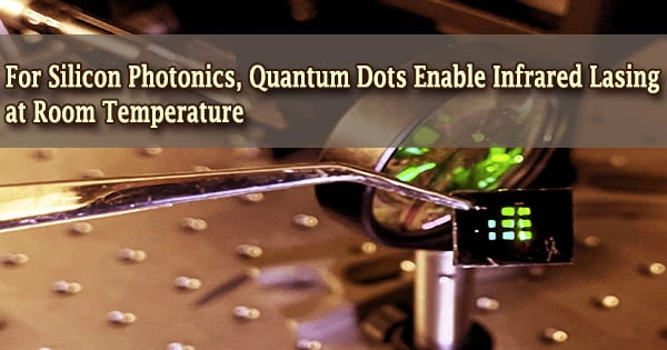
ICFO researchers Guy Whitworth, Mariona Dalmases, and Nima Taghipour, led by ICREA Prof. at ICFO Gerasimos Konstantatos, have reported the achievement of a colloidal quantum-dot-based infrared laser source operating at room temperature, compatible with CMOS technology, and tunable to emit in the telecommunications window, an important milestone needed for classical or quantum communications, in a recent paper published in Nature Photonic.
Prior to this discovery, the team had already completed an experiment that demonstrated stimulated emission and optical gain of quantum dots on thin films, but it lacked the ability to actually put this configuration into a cavity to accomplish lasing.
Infrared QD Lasing at room temperature
The researchers used a distributed feedback cavity (DFB) spincoated over a thin layer of PbS CQDs as the optical gain medium to select the best cavity for the experiment.
They demonstrated lasing emission across the eye-safe optical communication infrared spectrum and at room temperature by concomitantly tuning the size of the dots and the geometrical characteristics of the DFB to optimize the cavity resonance with the gain spectrum of the quantum dots, potentially finding the final piece of the jigsaw puzzle for silicon photonics.
Furthermore, the researchers went a step further and modified the surface of the dots to minimize electronic trap states and enhance stimulated emission. They were able to exhibit lasing emission at lower pumping intensities thanks to a robust doping of the quantum dots, paving the way for more practical applications.
As Prof. Gerasimos Konstantatos comments, “the results of this study are considered a major breakthrough in the field of CQD optoelectronics. This discovery may facilitate fully integrated silicon photonics, paving the way towards low-cost solution-processed and CMOS integrated lasing sources for on-chip comm or LIDAR applications. Prior to demonstrating lasing under continuous-wave or nanosecond stimulation, which is our next milestone, further work must be done to improve the material.”