At low temperatures, superconducting materials have zero electrical resistance, allowing them to conduct “supercurrents” without dissipation. A group of scientists led by Dr. Kazumasa Iida of Nagoya University in Japan recently developed a low-cost, scalable method for producing high-temperature superconductors using “grain boundary engineering” techniques. The new method could aid in the development of stronger, lower-cost, high-operating-temperature superconductors with significant technological applications.
Iron-based superconductors are iron-containing chemical compounds that were discovered to have superconducting properties in 2006. They were in the early stages of experimentation and implementation in 2008, led by newly discovered iron pnictide compounds (originally known as oxypnictides). (Previously, the majority of high-temperature superconductors were cuprates, with layers of copper and oxygen sandwiched between other substances (La, Ba, Hg).
This new generation of high-temperature superconductors appears to be based on conducting layers of iron and a pnictide (chemical elements in group 15 of the periodic table, typically arsenic (As) and phosphorus (P)).
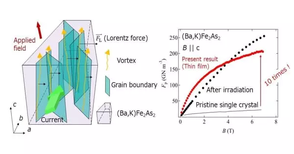
Crystalline materials are made up of ‘grains,’ which are different regions with different crystalline orientations. A ‘low-angle grain boundary (LAGB)’ occurs when the angle between the boundaries of different grains in a material is less than their critical angle, LAGBs contribute to magnetic flux pinning, which improves the superconductor’s properties.
Dr. Kazumasa Iida
A property is known as “pinning potential” is critical to the dissipation-free conduction of currents in superconductors in the presence of a magnetic field. Pinning describes how superconducting matrix defects pin vortices against the Lorentz force. Controlling the material’s microstructure allows for the careful introduction of defects into the material to form “artificial pinning centers” (APCs), which can then improve its properties. “Ion irradiation” is the most common method for introducing such defects into superconductors. Ion irradiation, on the other hand, is both complicated and costly.
Professor Iida and his research team successfully grew a thin-film superconductor with a surprisingly high pinning efficiency without the use of APCs in their study, which was published in NPG Asia Materials. “Crystalline materials are made up of ‘grains,’ which are different regions with different crystalline orientations. A ‘low-angle grain boundary (LAGB)’ occurs when the angle between the boundaries of different grains in a material is less than their critical angle, LAGBs contribute to magnetic flux pinning, which improves the superconductor’s properties” Dr. Iida explains.
FBS (iron-based superconductors) are thought to be the next-generation superconductor technology. Professor Iida and colleagues grew an FBS called “potassium (K)-doped BaFe2As2 (Ba122)” using a technique called “molecular beam epitaxy,” which involves growing the superconductor on a substrate. “The difficulties in controlling volatile potassium made realizing epitaxial K-doped Ba122 difficult, but we succeeded in growing the thin films on fluoride substrates,” says Dr. Iida.
The FBS was then characterized using transmission electron microscopy, and the team discovered that it was composed of columnar grains 30-60 nm wide. These grains formed LAGB networks after being rotated around the crystallographic principle axes by angles well within c for K-doped Ba122.
The electrical resistivity and magnetic properties of the thin film were then measured by the researchers. They discovered that the thin films had an unusually high critical current (the maximum current in a superconductor above which it transitions to a dissipation state). The LAGB networks also ensured that the material had a high pinning efficiency. “Our results show that the in-field properties of ion-irradiated K-doped Ba122 are comparable to those of ion-irradiated K-doped Ba122. Furthermore, grain boundary engineering is a straightforward technique that can be scaled up for industrial applications “Dr. Iida makes a comment.
The findings of this study could hasten the development of strong magnets based on superconductors, resulting in advances in magnetic resonance imaging (MRI). The high investment and operational costs of MRI machines due to the cooling costs of the superconductors within are currently limiting its widespread application. However, with simple and low-cost techniques like grain boundary engineering for superconductors, MRIs may become more accessible to patients, improving our quality of life.