A group of physicists at Purdue University created a device in 2018 that experimentally demonstrated quasiparticle interference in the fractional quantum Hall effect for the first time at filling factor v=1/3.
The Manfra Group has been able to broaden their study to include experiments that investigate counterflowing charged edge modes at the 2/3 fractional quantum Hall state because to the continued development of these heterostructures.
They have recently published their findings, “Half-Integer Conductance Plateau at the ν = 2/3 Fractional Quantum Hall State in a Quantum Point Contact,” in Physical Review Letters on February 17, 2023.
Dr. Michael J. Manfra, Bill and Dee O’Brien Distinguished Professor of Physics and Astronomy, Professor of Electrical and Computer Engineering, Professor of Materials Engineering, and Scientific Director of the Microsoft Quantum Lab West Lafayette lead the team.
The lead author of the publication is Dr. James Nakamura, senior research scientist. Dr. Geoffrey Gardner and graduate student Shuang Liang were also co-authors of this publication making valuable contributions to heterostructure growth.
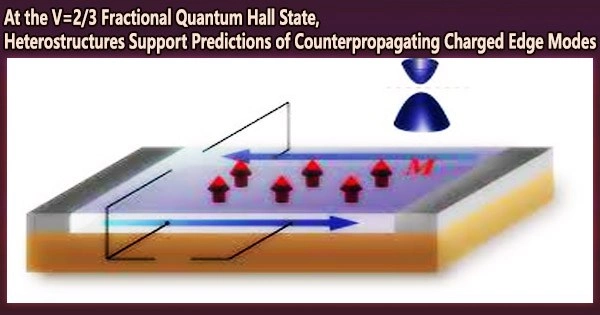
In the experiment, the group created a semiconductor material that has a two-dimensional electron strip in it. They constructed a 300 nanometer-wide quantum point contact on top of this semiconductor, which is made up of metal gates. They guided the conducting edge states through the small gap using the quantum point contact.
At a certain value of the magnetic field, the quantum Hall state is called the ν = 2/3 fractional quantum Hall state. At all quantum Hall states, electrical current is carried by edge states that flow around the edge of the sample, and they are chiral, meaning each edge state only flows in one direction (clockwise or counterclockwise). The ν = 2/3 state is predicted by theoretical physicists to have the special property that the there are two edge states which flow in the opposite direction to each other, one clockwise and the other counterclockwise. This is different from most quantum Hall states, where all the edge states flow in the same direction.
Dr. James Nakamura
They were able to measure an electrical conductance in this setup, as shown by the image above, that was half the value of e2/h. This experimental result is consistent with longstanding theoretical predictions for the edge states of the ν = 2/3 fractional quantum Hall state.
“We have a semiconductor structure that contains electrons arranged in a plane, called a two-dimensional electron system. When you cool the electrons down to low temperature and put them in a strong magnetic field, they form special states of matter called quantum Hall states,” explains Nakamura.
“At a certain value of the magnetic field, the quantum Hall state is called the ν = 2/3 fractional quantum Hall state. At all quantum Hall states, electrical current is carried by edge states that flow around the edge of the sample, and they are chiral, meaning each edge state only flows in one direction (clockwise or counterclockwise). The ν = 2/3 state is predicted by theoretical physicists to have the special property that the there are two edge states which flow in the opposite direction to each other, one clockwise and the other counterclockwise. This is different from most quantum Hall states, where all the edge states flow in the same direction.”
“We used a device with metal gates called a quantum point contact to control the edge states, and our measurements of the edge states in the quantum point contacts confirm the counterflowing edge states in our device. The quantum point contact brings the edge states on opposite edges of the sample close together. We measured a value of electrical conductance across the device equal to half of the value e2/h, where e is the electron’s charge and h is Planck’s constant. This value of the conductance is strong experimental evidence that our system has the edge structure with two counterflowing edge states.”
Due to the university’s cutting-edge capabilities for semiconductor growth, nanofabrication, and low temperature electrical measurements, this all-Purdue team of physicists is particularly positioned for success.
“A crucial aspect is the nanotechnology facilities at Purdue,” says Nakamura. “This includes the machine, called an MBE (molecular beam epitaxy) machine, which is used to produce the semiconductor structures. This very specialized machine, operated by the Manfra group, requires expertise to build and operate so this is an essential advantage at Purdue. Liang, under the guidance of Gardner, is responsible for this aspect of our work.”
“Additionally, the cleanroom in the Birck Nanotechnology Center is a state-of-the-art facility with a wide range of equipment available for us to use, that we used to fabricate the quantum point contact gates. Having all these resources and expertise available at one institution makes our experiments possible.”
This study is a component of a larger effort to comprehend and control fractionally charged anyons in the fractional quantum Hall domain, an excellent testbed for examining the effects of topology in condensed matter physics that could be utilized to build qubits.
The U.S. Department of Energy, Office of Science, Office of Basic Energy Sciences support this research, under award number DE-SC0020138.