A team of Northeastern University mechanical engineers was able to synthesize highly dense, ultra-narrow silicon nanowires that could revolutionize the semiconductor industry after a 10-year research study that began by accident and was met with skepticism. Their findings were published in Nature Communications.
Northeastern professor of mechanical and industrial engineering Yung Joon Jung says it was possibly his favorite research project. “Everything is new, and it took a lot of perseverance,” says Jung, who specializes in nanostructure system engineering and application and previously studied carbon nanotubes.
Jung and his colleagues, including another Northeastern mechanical engineering professor, Moneesh Upmanyu, have made significant advances in nanowire synthesis by discovering a new, highly dense form of silicon and mastering a new, scalable catalyst-free etching process to produce ultra-small silicon nanowires with diameters ranging from two to five nanometers.
Students brought Jung’s attention to an unusual result of an experiment they were conducting using silicon wafers about ten years ago. Jung claims that the material he saw under an electron microscope was not the one they intended to produce.
Jung claims that he decided to learn more about this substance and discovered that it was silicon with a “very, very tiny” wire-like nanostructure. He claims that they were able to replicate the new material, but when they tried to improve the synthesis process, the nanowires did not grow.
You want to understand the process so you can manipulate it to do what you want. They will also be looking for collaborators who are interested in developing devices using this new silicon material. You want a new version of something you created to be as widely adopted as possible. Commercialization and device integration, in my opinion, are critical here.
Upmanyu
The scientist and his team had to go back in time and study the synthesis mechanism as well as the material’s atomic-scale structure and properties from the beginning. Jung, an experimentalist, decided to enlist Upmanyu, who understands materials and explains experiments using theory, computer modeling, and simulation.
“I always need help from Moneesh to understand what is happening,” Jung says.
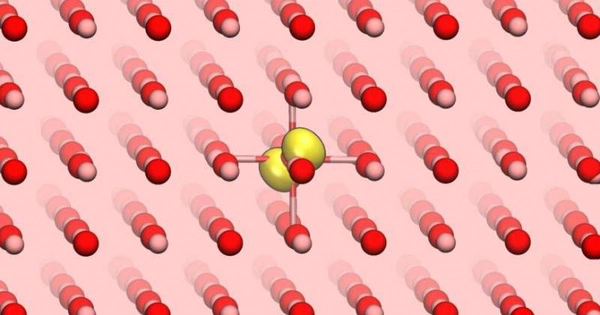
The scientists thought that maybe the substance resulting from silicon wafers during synthesis was not silicon at all. The material had a highly compressed structure, reduced by 10% to 20% compared to regular silicon, which normally is not stable in such a compressed state, Upmanyu says.
Some of their colleagues and research reviewers were of the same opinion. “They would say, ‘This shouldn’t be silicon’ or ‘This shouldn’t occur with silicon,'” Jung says. Through the computational analysis and modeling, Upmanyu was able to show that, despite unusual properties, the new material was a form of silicon with a very thin layer of oxide on top, which probably helps sustain the compression, he says.
“This material is very promising,” he says. “That compression, I feel, is at the heart of all the interesting properties you see.”

One of the reasons silicon is widely used as a semiconductor in microelectronics such as computer chips, integrated circuits, transistors, silicon diodes, and liquid crystal displays is that it is cheap and abundant, Upmanyu says. According to the Royal Society of Chemistry, it is the second most abundant element in the Earth’s crust after oxygen, but it does not occur in its pure, uncombined state in nature. It can be found in sand, quartz, flint, granite, mica, and clay, among other stones and minerals.
The thriving silicon computer chip industry even gave the southern region of San Francisco Bay a new name in the 1970s—”Silicon Valley,” which was popularized by Don Hoefler, an Electronic News Magazine reporter.
Traditional silicon, on the other hand, cannot withstand high temperatures and is thus limited to low-power applications. The bandgap is 1.11 electron Volts (bandgap determines the energy needed to make the electrons in the semiconducting material conduct electricity upon being stimulated by external sources).
The new material has an ultra-wide bandgap of 4.16 eV—a world record, Jung says. The ultra-wide bandgap implies that the material needs larger stimuli to conduct electricity, but can operate at high power, high temperature, and high frequencies. Silicon nanowires produced from this new material will be suitable for power electronics, transistors, diodes, and LED devices, Jung says.
Unlike regular silicon, the new material is highly resistant to oxidation. It is also photoluminant—able to emit blue and purple light, which can be used for ultraviolet lighting and in blue light diodes.
Jung and his research team have also created a new method of producing silicon nanowires, called chemical vapor etching, which removes material instead of growing crystals. As a result, they can make nanowires that are 10 to 20 times smaller than the silicon nanowires currently used commercially.
Catalyst particles are used in previously known nanowire synthesis processes to grow silicon crystals. “The catalyst-free aspect cannot be overstated enough,” Jung says, “because it eliminates the need to remove the catalyst after synthesis, which invariably degrades the functional properties of the nanowires.”
He claims that catalyst particles can become embedded in the nanowire surface and are nearly impossible to remove. Scientists can now create nanowires with controlled lengths of up to 100 microns.
“I feel a broad impact going forward,” Upmanyu says. “This chemical vapor etching method that he [Jung] has pioneered, is going to be useful for a host of other materials. You can think of not just electronic applications, but any application where you want to have a small-size dimension of a material made. It is very powerful.”
He believes that the new silicon material will be very appealing to the semiconductor industry. It has applications in military radios, radars, and photovoltaics such as solar cells. According to Upmanyu, regular silicon bandgap does not allow for the processing of ultraviolet light and its use in the generation of electricity.
“So, if you have a wide-bandgap material that is cheap and abundant, like silicon,” he says, “you can now have very high-efficiency solar cells.” It can even be used to harvest solar energy while submerged. Water absorbs the red and infrared spectrums, so solar cells that can harvest blue and ultraviolet light are critical, according to Upmanyu.
The new silicon nanowires can improve lithium-ion batteries, Jung says. Further adding some select materials like phosphorus or nitrogen (a technique called doping) can lead to other interesting properties and allow other applications, Upmanyu says.
Because of their small size, he believes that various interesting quantum phenomena can be manipulated in these silicon nanowires, making this material promising for quantum information processing and possibly even quantum computing, says Upmanyu.
Several other engineering institutions from around the world, including Korea Institute of Science and Technology, Korea Advanced Institute of Science and Technology, Tokyo University of Science, University of Science and Technology of China, and Rensselaer Polytechnic Institute in New York, contributed to this research.
The investigation is not finished. Scientists are still interested in better understanding all of the chemistry involved in the process and determining why the compression of this form of silicon is so stable. They want to improve the etching process to produce a smoother surface and scale it up for industrial use.
“You want to understand the process so you can manipulate it to do what you want,” Upmanyu says. They will also be looking for collaborators who are interested in developing devices using this new silicon material. “You want a new version of something you created to be as widely adopted as possible. Commercialization and device integration, in my opinion, are critical here” According to Upmanyu.