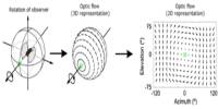
On sports broadcast stations, a slow-motion video depicts actions in hundredths of a second. In contrast, nanoscale processes occur in the so-called femtosecond range: As an illustration, it takes an electron just billionths of a second to orbit a hydrogen atom.
Specialized equipment is being used by physicists all over the world to film these incredibly quick nano-processes. Researchers at Kiel University (CAU) have created a fresh approach for studying such films that is based on a different physical idea and offers more precise and extensive alternatives for research.
They did this by combining an electron microscope with metallic thin sheets with nanostructures that produce brief light pulses. Hence, they were able to capture on film, in a first experiment, the coherent interactions between light and electrons in a semiconductor. Their results are published in Nature Physics.
New method is simpler and more cost-effective
Up until recently, high-power lasers and electron microscopes have typically been used to create videos of ultrafast nano-processes. But only a small number of research teams can afford the expensive and elaborate settings.
“Our concept does not require expensive and complicated lasers and can be easily replicated,” says Nahid Talebi, Professor of Experimental Physics at the CAU.
In an electron microscope, a beam of electrons is bundled, accelerated, and pointed at a sample of material. Conclusions regarding the characteristics of the materials and internal processes can be drawn based on how the electrons traverse the sample or are reflected.
If a short time later the slower electron beam also hits the semiconductor sample, we can see from the reaction of the electrons how the excitons have behaved in the meantime.
Professor Nahid Talebi
“Electron microscopes have a significantly better spatial resolution than optical microscopes and make investigations in the nanometer range possible in the first place,” says Talebi.
It is pretty simple to enhance the temporal resolution of electron microscopes and transform them into their ultrafast counterparts thanks to the unique components she has created. Now, without the use of lasers, nanoscale processes can also be recorded in ultrafast films on the femtosecond time scale.
With her new publication, Talebi not only demonstrates that her method works. Together with her research associate Dr. Masoud Taleb, she also provides experimental evidence for coherent interactions of photons and electrons in a semiconductor, which had previously only been described theoretically.
The quantum material tungsten diselenide, WSe2, used for this purpose originates from a collaboration with Professor Kai Rossnagel within the priority research area KiNSIS (Kiel Nano, Surface and Interface Science) at Kiel University.
Nano-structured metal generates short light pulses
A particular nanostructure that resembles a kitchen sieve is a key element of Talebi’s idea. It can be inserted into an electron microscope, where it functions like a light source, called “EDPHS” (electron-driven photon source). This metal structure is struck by an electron beam, and the hole pattern produces focused, brief light pulses that can be utilized to create quick films.
Researchers punched extremely small holes, ranging in size from 25 to 200 nanometers, into a thin gold foil to produce the unique structure. Because the light pulses only happen when a specific hole pattern is present, Talebi has precisely determined the sizes and distances. The “nanosieves” were produced in close collaboration with Dr. Mario Hentschel from the research group of Prof. Harald Giessen, University of Stuttgart.
Together with colleagues from Amsterdam, Talebi had previously modified the electron microscope so that it can detect cathodoluminescence. These light signals are generated when fast electrons hit metal.
Interactions between electrons and photons documented in films
The brief light pulses from the sieve-like nanostructures hit the semiconductor sample at the speed of light in the experiment described in the current research. Here they excite excitons, so-called quasiparticles.
These are electrons that have detached themselves from an atom and are still coupled to the hole they created (“electron-hole pairs”).
“If a short time later the slower electron beam also hits the semiconductor sample, we can see from the reaction of the electrons how the excitons have behaved in the meantime,” explains Talebi.
A coherent interaction between electrons and photons can be seen in the cathodoluminescence signals that are produced by superimposing an electron beam and light pulses.
The researchers also included a piezoelectric crystal in the microscope setup to be able to video these phenomena. This enables them to precisely alter the distance in space between the light source and the sample, and consequently, the interval in time between the incident light pulses and the electrons.
“In this way, images can be taken at different stages of the process and assembled into a film,” Talebi summarizes.