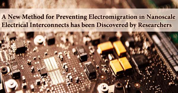
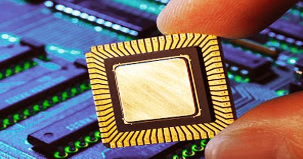
Researchers at the University of South Florida recently devised a unique method for preventing electromigration in nanoscale electronic interconnects, which are common in today’s integrated circuits. This was accomplished by covering copper metal interconnects with hexagonal boron nitride (hBN), an atomically thin two-dimensional (2D) insulating material with a structure akin to the “wonder material” graphene.
Electromigration occurs when an electrical current passes through a conductor and causes atomic-scale material degradation, eventually leading to device failure. A barrier or liner material is employed in conventional semiconductor technology to overcome this problem, but this takes up valuable space on the wafer that could otherwise be utilized to pack in more transistors. It was discovered more than a century ago, but it wasn’t until the very harsh conditions required for integrated circuit functioning made it painfully evident that it became a problem.
Although electromigration occurs whenever current passes through a metal wire, the circumstances required for electromigration to be a problem did not exist at the time. Only a research scientist, and only with extreme effort, could run enough current through a bulk metal wire to study the effects of electromigration. As a result, for at least a century, electromigration was a fascinating topic in solid state physics, intriguing grist for university research mills, but of no economic importance.
Michael Cai Wang, a USF mechanical engineering assistant professor, uses the world’s thinnest materials, two-dimensional (2D) materials, to achieve the same aim.
“This work introduces new opportunities for research into the interfacial interactions between metals and ångström-scale 2D materials. One of the outcomes of this study is improved electrical and semiconductor device performance. The outcomes of this study offer up new possibilities for semiconductor and integrated circuit fabrication in the future,” Wang said. “Our novel encapsulation strategy using single-layer hBN as the barrier material enables further scaling of device density and the progression of Moore’s Law.”
An ångström is one-tenth of a nanometer, while a nanometer is 1/60,000 of the thickness of human hair. Manipulation of such tiny 2D materials necessitates high accuracy and precise handling. The current method for preventing electromigration is to guarantee that cables with high current density have adequate diameters to support them. A thinner wire may be able to hold a higher current density than a broader one due to chemical-mechanical polishing (CMP) processes that reduce wire thickness.
For a wire with a high current density, there might be many ranges of EM compatible widths. EM compliance widths are generally calculated using current density tables. Copper interconnects passivated with a monolayer hBN via a back-end-of-line (BEOL) compatible approach exhibited more than 2500 percent longer device lifetime and more than 20% higher current density than otherwise identical control devices, according to a recent study published in the journal Advanced Electronic Materials.
This enhancement, along with hBN’s ngström-thinness relative to traditional barrier/liner materials, enables for even more integrated circuit densification. These discoveries will aid in improving gadget efficiency and lowering energy usage.
“With the growing demand for electric vehicles and autonomous driving, the demand for more efficient computing has grown exponentially. Better ASICs (application-specific integrated circuits) adapted to these growing sustainable energy demands will be possible because to the promise of increased integrated circuit density and efficiency.” explained Yunjo Jeong, an alumnus from Wang’s group and first author of the study.
Hundreds of microelectronic components make up the ordinary contemporary automobile, and the importance of these little but vital components has been underlined by the recent global chip shortage. Improving the efficiency of the design and manufacture of these integrated circuits will be critical in preventing future supply chain disruptions. Wang and his students are currently looking at methods to speed up their procedure so that it may be used on a larger scale.
“Our findings are not limited only to electrical interconnects in semiconductor research. The fact that we were able to achieve such a drastic interconnect device improvement implies that 2D materials can also be applied to a variety of other scenarios.” Wang added.